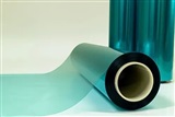
Asahi Kasei, a Japanese multinational chemical company, has announced a significant investment to increase photoresist film production capacity at a plant in Taiwan. The move aims to meet the growing demand for advanced packaging of chips used in artificial intelligence systems.
Photoresist films are key materials in semiconductor packaging processes. They are not used to print transistors on wafers—that is the domain of lithographic photoresists—but come into play in the encapsulation and interconnection phase: redistribution layers (RDL), interposers, high-density substrates. In short, they enable multiple chips to be connected in a single package, boosting bandwidth and reducing power consumption.
Packaging has become a decisive competitive factor. Technologies such as fan-out, chiplet integration, and HBM memory integration depend on thin films with precise dielectric properties and mechanical strength. Asahi Kasei is not the only player, but its expansion in Taiwan—close to giants like TSMC and ASE—signals a broader capacity ramp to keep pace with demand for GPUs, accelerators, and custom AI ASICs.
Those building on-premise infrastructure for LLM inference and training watch these developments closely: denser, better-interconnected chips translate into higher compute performance per watt and per euro spent. The total cost of ownership (TCO) of an inference cluster is influenced by how efficiently silicon handles memory and communication. If the packaging supply chain strengthens, the accelerator market could benefit from greater availability and, over time, less volatile pricing.
Of course, expanding a film production line does not single-handedly shorten GPU lead times, but it is one piece of a complex ecosystem—from chemistry to foundry—that today determines how quickly AI can move from the cloud to local data centers. For those evaluating on-premise deployment, AI-RADAR provides analytical frameworks to compare TCO, latency, and hardware constraints.





💬 Comments (0)
🔒 Log in or register to comment on articles.
No comments yet. Be the first to comment!