
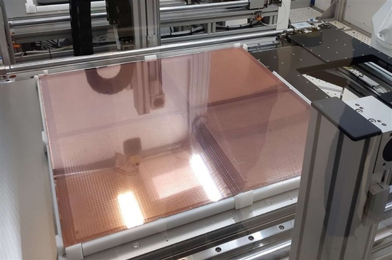
Chinese semiconductor equipment maker Circuit Fabology Microelectronics Equipment (CFMEE) has announced its first order for a large-format PLP (Panel Level Packaging) lithography system, purpose-built for AI chip packaging. The news, sparse in itself, is a structural signal: the center of gravity of advanced manufacturing for AI is shifting, and the implications go well beyond the business headline.
PLP is a packaging technique that replaces traditional circular wafers with larger rectangular panels, increasing the number of chips processed per cycle and reducing unit costs. For AI chips — GPUs, accelerators, HBM interposers — packaging has become a bottleneck as critical as front-end lithography. Having a new supplier capable of offering large-format panel lithography opens a diversification opportunity in a market dominated by very few players.
That CFMEE, a company that until recently operated mostly in the Chinese domestic market, is now landing international orders for AI applications says a lot about the sector’s technological maturation. This is no longer about producing basic components, but about supplying key tools for advanced assembly. In practice, those who until yesterday bought machinery from established vendors can now look to Beijing (or Shanghai) to equip 2.5D and 3D packaging lines.
Why packaging lithography shifts the balance
When discussing LLM infrastructure, attention often focuses on GPU supply or software optimization. Yet the real bottleneck lies in the ability to package increasingly complex chips, with high-density interconnects and extreme thermal loads. Without efficient packaging, promises of low-latency on-premise inference remain on paper. Large-format PLP intervenes exactly here: it enables multi-die projects and integrated memory modules, reducing assembly time and improving yield.
For those evaluating self-hosted deployment of large models, the availability of accelerated hardware is not a given. Every element that diversifies the supply chain — and potentially lowers costs for equivalent performance — directly impacts mid- to long-term planning. In this sense, the entry of a new panel lithography equipment maker is not just industry news, but a piece of the puzzle that could make on-premise clusters economically sustainable on a larger scale.
Technological sovereignty and parallel supply chains
There’s a second reading, tied to data sovereignty and the geography of production. While Europe and the United States invest in chip fabs, China is accelerating across the entire equipment supply chain. Having lithography capability for advanced packaging means being able to offer integrated solutions to markets that, for geopolitical or compliance reasons, prefer to diversify suppliers. It’s no coincidence that CFMEE stresses the AI purpose of the device: the company aims to capture demand for data center and server chips — the very hardware that powers on-premise workloads.
This dynamic intersects the choices of those implementing LLMs in air-gapped or bare-metal environments for privacy reasons. Knowing that a parallel supply chain of packaging equipment exists weakens the leverage of the few incumbents and, over time, can help moderate the total cost of ownership (TCO) of inference infrastructure. Numbers are not yet on the table, but the direction is clear: packaging becomes a field of technological and commercial competition, with direct consequences for those sizing and procuring AI hardware.




💬 Comments (0)
🔒 Log in or register to comment on articles.
No comments yet. Be the first to comment!