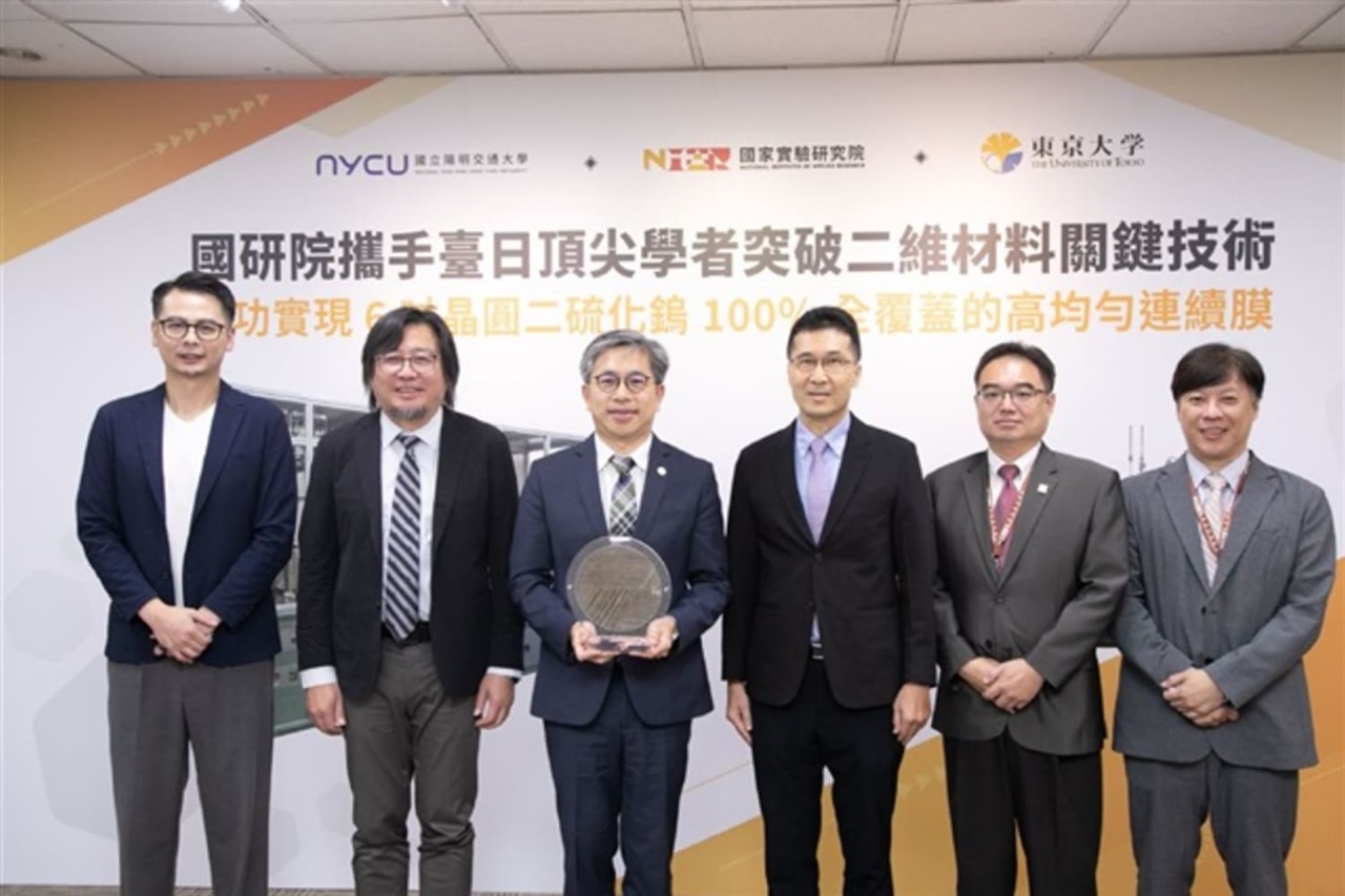
When silicon becomes a physical limit, innovation shifts to materials chemistry. That is the message coming from Taiwan, where TSMC, ASML and Imec have laid the groundwork to bring chips based on 2D materials from the lab to mass production within five years.
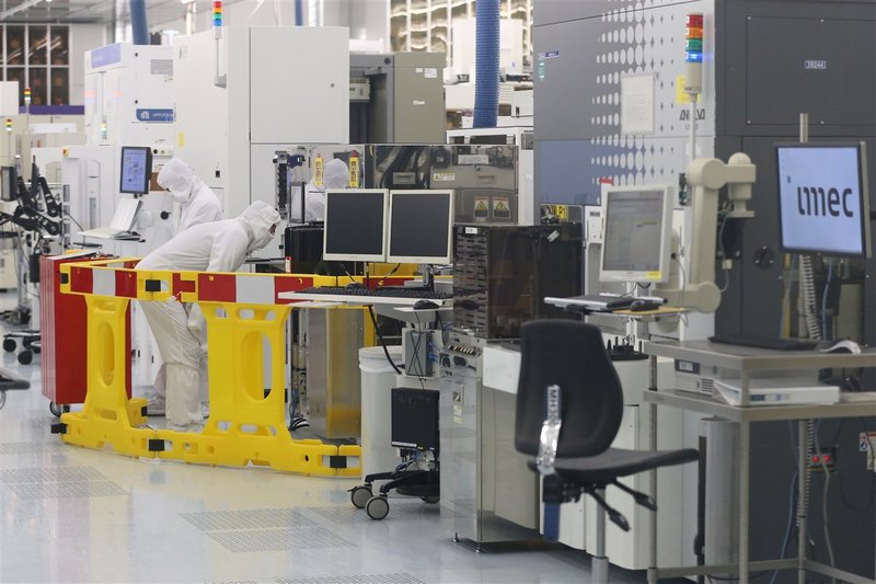
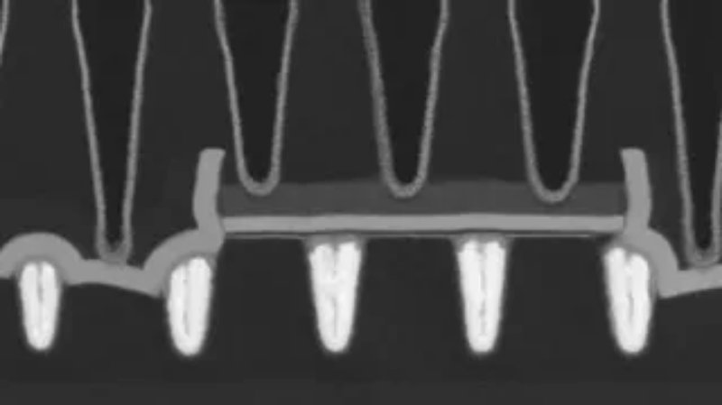
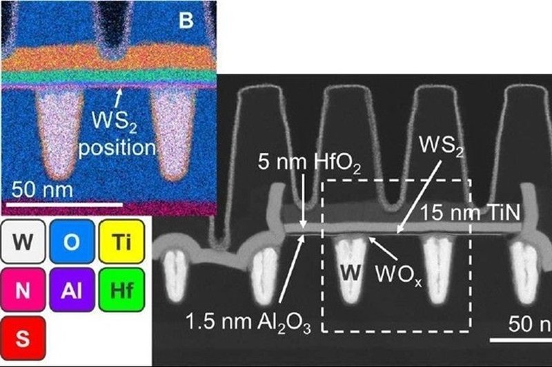
2D materials – transition metal dichalcogenides such as molybdenum disulfide, or graphene – are atomic layers with electronic properties that could, in the long run, surpass silicon. They allow the construction of transistors with channels just a few atoms thick, dramatically reducing power dissipation and paving the way for integration densities unattainable with today’s gate-all-around FinFETs. But turning a laboratory monolayer into a reliable process on 300 mm wafers is a challenge that demands a complete ecosystem: transistor design (Imec), the lithography machine capable of aligning patterns at those scales (ASML with its high-NA EUV scanners), and the ability to integrate everything at industrial volumes (TSMC).
For those managing on-premise infrastructure for LLMs and inference workloads, this triangulation carries significant weight. Near-future chips based on sub‑2 nm nodes will keep squeezing silicon at ever-increasing energy per transistor. The shift to 2D materials, by contrast, promises an efficiency leap that could structurally lower the TCO of self-hosted deployments. In a scenario where data sovereignty forces models to be kept within the corporate perimeter, computational density and the performance-per-watt ratio become the decisive variables. A rack of GPUs or accelerators built on 2D transistors could deliver the same inference capacity as today’s cluster at a fraction of the energy, making air-gapped deployments economically viable for organizations that now consider them a luxury.
The most disruptive aspect is the choice of Taiwan as the manufacturing epicenter. This is not just an industrial move: in a geopolitical landscape where semiconductor supply chains are strategic weapons, this collaboration confirms that the center of gravity for silicon – and now for post-silicon – remains the island. For European and American companies investing in domestic production capacity (such as through the CHIPS Acts), the TSMC-ASML-Imec project raises the bar: it signals that the next transistor generation will not emerge from new fabs built elsewhere but will consolidate where a mature ecosystem already exists. This carries direct implications for technological sovereignty: those who depend on foreign hardware for on-premise AI will face an even more concentrated supply node.
On the research front, Imec’s involvement is the litmus test. The Belgian center is not a supplier but a process enabler; its presence alongside TSMC and ASML suggests that the route to 2D chips requires a transfer of know-how in metrology and materials integration that only an independent body can orchestrate. It remains to be seen whether this convergence will truly accelerate time-to-market, or whether timelines will lengthen due to the complexity of retrofitting existing fabs. What is certain is that the angstrom race is no longer just about scale pitch: now the game is played on the periodic table.



💬 Comments (0)
🔒 Log in or register to comment on articles.
No comments yet. Be the first to comment!