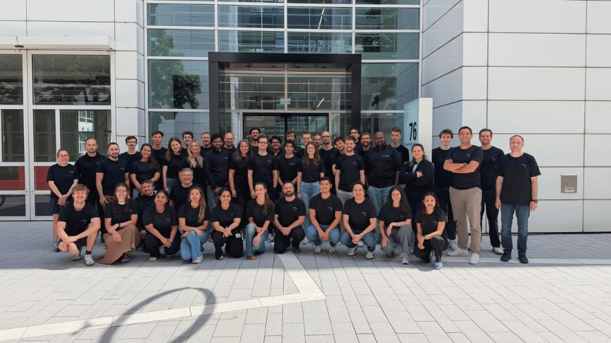
Brussels just placed a €91 million bet on a very unusual microscope. It doesn’t use traditional optical lenses, but atomic defects in diamond crystals. QuantumDiamonds, a three-year-old startup spun out of the Technical University of Munich, wants to turn this principle into a metrology tool capable of hunting down hidden defects in next-generation semiconductors.
The stakes are not only technical. Europe consumes about a fifth of the world’s chips but makes only a tenth of them. That gap translates into dependence on external suppliers and, in the era of Large Language Models, into waiting lists for the GPUs and accelerators needed to run inference on-premise. Any tool that promises to boost chip fab yields – by reducing failures and improving wafer quality – directly affects those who today evaluate self-hosted stacks for data sovereignty or TCO reasons.
The technology relies on nitrogen-vacancy (NV) centers in diamond, one of the most studied quantum systems for sensing. When illuminated with green light, these defects emit photons whose intensity is sensitive to local magnetic fields. By bringing the diamond close to an integrated circuit, the microscope maps currents and weaknesses without contact, spotting internal short circuits or anomalies that escape electrical testers. This is not science fiction: academic groups have used it for years to analyze memories and transistors. QuantumDiamonds’ challenge is to turn a laboratory experiment into an industrial machine that operates in a cleanroom at the speed required by mass production.
The analogy with ASML, called up by the fundraising’s title, is not far-fetched. ASML became dominant not by making chips, but by supplying the hardware – EUV lithography machines – without which chips cannot be printed at the most advanced nodes. QuantumDiamonds is aiming for a similar role in inspection and metrology, an increasingly critical link in the supply chain. With the shift to chiplets and 3D stacking, hidden defects in vertical interconnects or micro-bumps become an invisible threat. Checking a single die is not enough: you need to verify the entire assembly, and traditional optical tools are starting to show their limits. A quantum sensor based on diamond comes into play precisely where the signals to be captured are magnetic, thermal, or electrical on a sub-micrometric scale.
For those building AI infrastructure, the news has a tangible side. Every extra percentage point of yield in a leading-edge fab means more GPUs available for the same number of processed wafers, less waste, and, hopefully, a less squeezed market. At a time when on-premise inference requires specialized hardware – from H100s to PCIe-based systems that push VRAM limits – production capacity remains the real bottleneck. Designing lighter LLMs in INT8 or FP8 quantization helps only so much if the hardware to run them on is nowhere to be found or arrives months late.
The move also signals a structural shift in how Europe is trying to carve out a role in the semiconductor game. Rather than chasing giants like TSMC or Samsung on the foundry side, which demands tens of billions in investment, Brussels is funding companies that can become champions in equipment. It’s a strategy reminiscent of ASML’s origins, born when Dutch and German governments backed research on ultraviolet lithography even though they had no major chip fab on their territory. Today ASML is worth more than €300 billion. Betting on QuantumDiamonds means imagining that, over the next ten years, every advanced process node fab will need at least one of these microscopes, and that the intellectual property stays in European hands.
Granted, the road is long. From prototype to a tool qualified for 24/7 production takes years, and the metrology market is already guarded by Applied Materials, KLA, and Hitachi High-Tech. But the fact that a large part of the funding comes from European public funds suggests that the bet goes beyond the single product: it’s about building quantum sensing capabilities that tomorrow may also apply to biomedical sensors or navigation systems, creating a cross-benefiting ecosystem.
For those who today need to decide between buying an on-premise cluster or subscribing to a cloud service, none of this changes the immediate choice, but it does affect the future cost of hardware. More fast and precise inspection tools mean more good chips per wafer, lower unit costs, and, over the long run, greater accessibility of the GPGPUs needed to run ever-larger models locally. This is the kind of dynamic that plays out far from benchmarks and frameworks, but that defines the real availability of the raw material of artificial intelligence.








💬 Comments (0)
🔒 Log in or register to comment on articles.
No comments yet. Be the first to comment!