Introduction
ASML stands as a silent yet fundamental pillar of the global technology industry. Without its lithography machines, the production of advanced chips, which power every modern device from smartphones to AI servers, would be impossible. ASML's technological roadmap is not merely an engineering exercise; it's a forecast of the future of computing capabilities. Each step forward in lithography translates into smaller, denser transistors, which in turn enable the creation of more powerful and efficient processors.
This impact is particularly felt in the artificial intelligence sector, where the demand for computational power for Large Language Models (LLMs) is constantly growing. The ability to produce high-performance chips with reduced power consumption is a decisive factor for the adoption and efficiency of AI systems, whether in the cloud or in self-hosted environments.
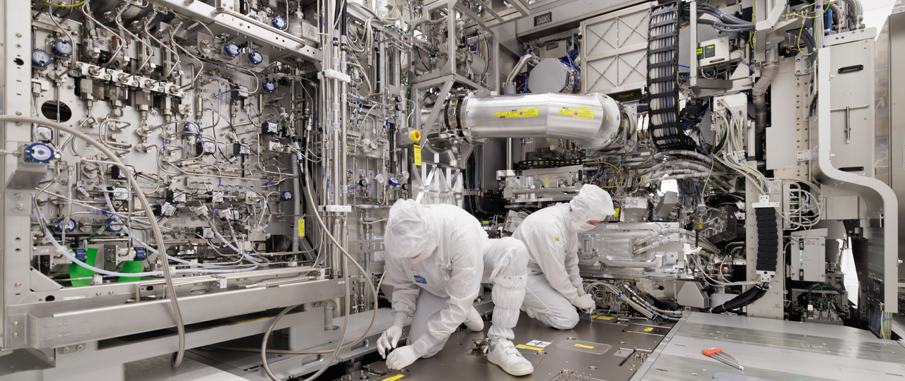
The Heart of Manufacturing: DUV, EUV, and Beyond
Lithography is the process by which circuits are "printed" onto silicio. ASML has led the evolution of this technology through several generations. Initially, DUV (Deep Ultraviolet) lithography allowed for increasingly smaller process nodes. However, to overcome the physical limits of deep ultraviolet light, EUV (Extreme Ultraviolet) lithography was developed.
Machines like the Twinscan EUV represent the pinnacle of this engineering, using an extremely short wavelength of light to create incredibly detailed patterns on silicio wafers. ASML's roadmap does not stop at current EUV but explores variants such as Low-NA, High-NA, and even Hyper-NA, each promising to push the boundaries of miniaturization further. These developments are crucial for transistor density and, consequently, for the ability to integrate more compute cores and VRAM into next-generation GPUs.
Implications for On-Premise AI
For organizations considering the deployment of LLMs in self-hosted or air-gapped environments, the evolution of lithography has direct implications. The availability of more performant chips means being able to run larger or more complex models with higher throughput and lower latency, all within their own infrastructure. This is fundamental for maintaining data control and ensuring compliance, which are priority aspects for many CTOs and infrastructure architects.
More efficient hardware, made possible by ASML's advancements, can reduce the Total Cost of Ownership (TCO) of on-premise AI systems, balancing initial investment with lower long-term operational costs. The increased compute density per unit of space and power allows for optimizing datacenter resource utilization, a critical factor for those managing local infrastructures. For those evaluating on-premise deployments, significant trade-offs exist between initial costs, scalability, and control, and AI-RADAR offers analytical frameworks on /llm-onpremise to evaluate these options.
Future Prospects and Challenges
The race for silicio miniaturization is far from over. ASML's roadmap indicates a continuous commitment to innovation, with the goal of overcoming the physical and engineering challenges that arise with each new process node. These efforts not only ensure that the semiconductor industry can continue to provide the fundamental building blocks for the digital age but also that the artificial intelligence ecosystem can rely on a constant stream of increasingly capable hardware.
For technical decision-makers, understanding these dynamics is essential. Deployment choices for AI workloads, particularly those prioritizing data sovereignty and on-premise control, are intrinsically dependent on the industry's ability to deliver cutting-edge silicio. ASML's innovation is, in this sense, a barometer for the future direction of AI infrastructure.


💬 Comments (0)
🔒 Log in or register to comment on articles.
No comments yet. Be the first to comment!