A New Approach to Energy Efficiency in AI Sensors
The artificial intelligence landscape is constantly evolving, with a growing demand for solutions that can operate efficiently outside traditional cloud data centers. A critical aspect for AI deployments, particularly on-premise and at the edge, is energy consumption, which is closely linked to the Total Cost of Ownership (TCO) and operational sustainability. In this context, the search for new hardware architectures that reduce energy requirements is of paramount importance.
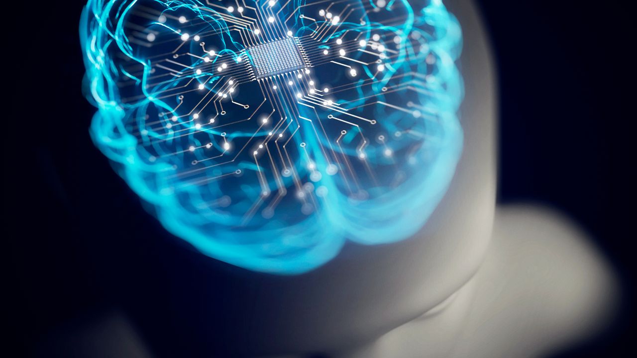
Recently, researchers have presented an innovative memory device inspired by the structure of the human brain. This development is specifically aimed at AI sensors and promises to significantly improve energy efficiency. The primary goal is to address one of the most persistent challenges in modern computing: the "memory wall," which is the bottleneck caused by the continuous movement of data between processing units and memory.
Integrating Sensing, Memory, and Processing in a Phototransistor
The core of this innovation lies in a phototransistor device that integrates light sensing, memory, and processing functionalities within a single unit. Traditionally, these functions are handled by separate components, which requires constant data transfer between them. This continuous movement of information not only introduces latency but is also one of the main causes of energy consumption in computational systems.
The approach proposed by the researchers aims to overcome this limitation by combining the three functionalities. As a phototransistor, the device is capable of directly perceiving light, processing it, and storing the results, drastically reducing the need to move data. This architecture, reminiscent of neuromorphic computing principles, allows processing to be performed directly where data resides or is generated, minimizing the energy expenditure associated with transfer.
Implications for On-Premise and Edge AI Deployments
The impact of such a device on energy efficiency is particularly relevant for on-premise and edge AI deployments. In these scenarios, energy resources can be limited, and TCO is a key metric for evaluating solutions. The ability of an AI sensor to process data locally, with reduced power consumption, opens new possibilities for applications in contexts such as industrial IoT, smart surveillance, and autonomous systems.
Reducing data movement not only translates into lower energy consumption but can also improve throughput and reduce latency, crucial factors for real-time AI applications. For companies evaluating self-hosted alternatives to cloud solutions for AI workloads, the emergence of specialized hardware like this offers new opportunities to optimize their infrastructures, ensuring greater control, data sovereignty, and lower operating costs. AI-RADAR offers analytical frameworks on /llm-onpremise to evaluate the trade-offs between different deployment strategies.
Future Prospects for AI Hardware
This development represents a significant step forward in the search for more efficient hardware architectures for artificial intelligence. Although still in research, the concept of integrating sensing, memory, and processing into a single component has the potential to profoundly influence the design of future AI chips and systems. The direction is clear: moving away from traditional computational models to embrace solutions closer to brain function, where processing is intrinsically linked to memory.
Continuous innovation in hardware is essential to unlock new capabilities and make AI more accessible and sustainable. Devices like this phototransistor could one day power a new generation of smart sensors, capable of operating with unprecedented energy autonomy, pushing the boundaries of AI towards increasingly pervasive and decentralized applications.


💬 Comments (0)
🔒 Log in or register to comment on articles.
No comments yet. Be the first to comment!