
Fifteen million in equity and another seventy-six in state aid: the round announced today by QuantumDiamonds puts €91 million into scaling a technology that starts with diamonds and aims to change how the semiconductor industry finds defects. The startup — founded in 2022 from the Technical University of Munich — does not make chips; it builds testing tools based on quantum sensors. Its stated goal is to plug into fabs worldwide, beginning with facilities already running in the United States and Taiwan.
The equity funding is led by climate-tech investor World Fund, with Bayern Kapital and existing backers IQ Capital, Earlybird, First Momentum, UnternehmerTUM, Creator Fund, and Onsight Ventures joining. The non-dilutive public portion comes from Germany’s Federal Ministry for Economic Affairs and the Free State of Bavaria, and it was approved last month by the European Commission. This arrangement avoids equity dilution and ties the company to work with SMEs, universities and research institutions.
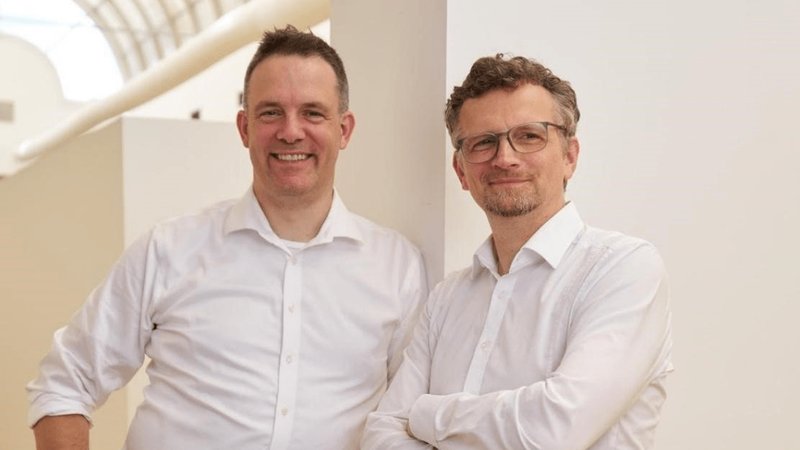
At the heart of the plan is a new high-tech testing facility in Munich, which QuantumDiamonds describes as a decisive piece of Europe’s push to produce its own technology components and software, reducing dependence on the United States. CEO and co-founder Kevin Berghoff is blunt: «Leading chipmakers see our technology as essential for solving yield challenges that today’s systems can’t address.»
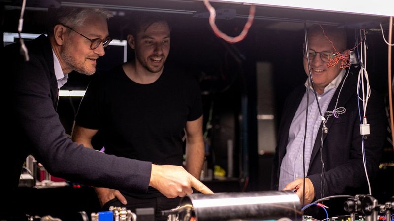
From a technical standpoint, quantum sensing using nitrogen-vacancy centers in diamonds promises to detect failures and defects at scales that conventional optical or electrical techniques miss. For those tracking the AI hardware market, the link isn’t immediate, but it’s structural. Every advanced chip — including the GPUs that run large language models in on-premise data centers — depends on high manufacturing yields. Better testing accelerates validation cycles, cuts waste and, for a given process node, increases the number of functional dice per wafer. At a time when demand for inference accelerators is soaring and supply-chain bottlenecks remain tight, any tool that lifts yields helps ease costs and makes on-premise deployments less constrained by silicon availability.
The move fits a wider picture. The European Union is pushing via the Chips Act and related legislation to build a continental semiconductor ecosystem, from raw silicon to finished hardware. Placing an advanced testing hub in Munich, rather than relying entirely on non-EU partners, is not just industrial policy — it’s a piece of digital sovereignty. Having domestic testing capability means components can be validated under European regulations without shipping wafers to Asia or the US. For those designing AI infrastructures with data-residency requirements and supply-chain audits, locally tested and certified chips add a layer of control that cloud-only solutions cannot offer.
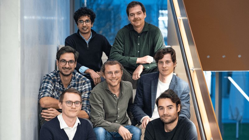
The company currently employs 70 people and expects to more than double its engineering team over the next twelve months. It already operates across Europe, Asia and the United States, with serial production ramping up. The total €91 million — injected in a framework where the state takes no equity — signals that public and private capital converge when the stakes are the physical supply chain of digital innovation. This is not a story about generative models, then, but about the material infrastructure without which those models remain pure abstraction.






💬 Comments (0)
🔒 Log in or register to comment on articles.
No comments yet. Be the first to comment!