
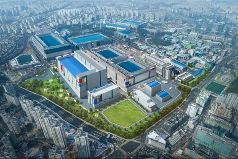
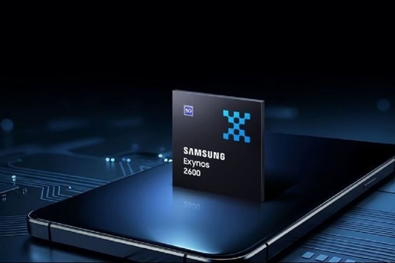
Samsung’s 2-nanometer node is becoming a magnet for custom silicon heavyweights, but the Korean foundry is starting to feel the weight of demand. According to rumors from Asian press, Samsung Electronics is evaluating whether to outsource the back-end design phase of the Tensor Processing Units (TPUs) it manufactures for Google. In practice, the chip’s physical design—place-and-route, timing closure, and layout verification—could be handed over to external design service companies, freeing internal resources to focus on manufacturing alone.
This is not an arcane detail. The back-end is where architectural choices collide with transistor reality: an exquisitely sensitive phase that determines clock frequencies, power consumption, yield, and ultimately the cost per chip. Handing it to a third-party partner means relinquishing granular control that, on such advanced nodes, can make the difference between competitive silicon and a design that struggles to scale.
The move, still under consideration, comes as demand for the 2 nm Gate-All-Around (SF2) process intensifies. Google is a marquee customer of Samsung Foundry for custom AI chips, deployed extensively in Google Cloud data centers for training and inference of Large Language Models like Gemini. But it is not alone: other hyperscalers and fabless players are knocking on Korea’s 2 nm door, creating a bottleneck not just in production capacity but also in engineering design talent.
What does this mean for the AI hardware landscape? In a market where the availability of high-performance accelerators dictates the roadmaps of enterprises and research labs, every supply-chain hiccup cascades downstream. If Samsung scales back its involvement in TPU physical design, Google faces a double risk: potentially longer development cycles and a less optimized chip versus target specifications. Rumors already swirl that future TPU production could partially migrate to TSMC’s 3 nm nodes, and a Samsung retreat from the design phase could accelerate that transition, cementing the Taiwanese giant’s near-monopoly on leading-edge process technologies.
For the AI accelerator ecosystem, greater concentration around TSMC is not welcome news. Less foundry competition means less bargaining power for customers, longer lead times, and higher price margins. In a scenario where organizations are evaluating on-premise deployment of ever-larger models—driving demand for specialized hardware like NVIDIA H100/H200 GPUs or proprietary ASICs—the robustness and diversification of the chip supply chain become strategic factors. Samsung’s move is a warning shot: even a manufacturing giant can be forced to choose between competing priorities, and when design resources run thin, AI silicon production can become an obstacle course.
It remains to be seen whether the back-end partners selected by Samsung can rise to the challenge of a 2 nm GAA process, which inherently requires re-engineered libraries and verification flows. If successful, the approach could become a model for handling the surge in custom projects without overloading internal teams. If not, the message will be clear: the race to the most advanced nodes is straining not only lithography machines but also the teams that turn architectures into working silicon.





💬 Comments (0)
🔒 Log in or register to comment on articles.
No comments yet. Be the first to comment!