Revolution in Chip Production: Nanoimprint Lithography Claims 90% Cost Reduction
A Chinese startup has announced a significant breakthrough in photonic chip production, claiming to have developed a process that bypasses traditional Deep Ultraviolet (DUV) lithography. This innovation, based on nanoimprint lithography, promises to cut production costs by up to 90%, opening new perspectives for the semiconductor industry and, by extension, for AI infrastructure.
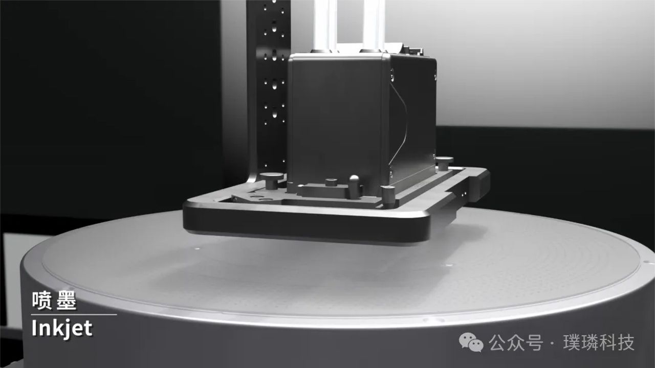
The ability to produce 8-inch wafers without resorting to complex and expensive conventional optical lithography techniques represents a potential game-changer. For companies evaluating the deployment of AI workloads, particularly Large Language Models (LLM), on self-hosted or on-premise infrastructures, reducing hardware costs is a critical factor in calculating the Total Cost of Ownership (TCO).
Nanoimprint Lithography: A Technical Deep Dive
DUV lithography has been the backbone of semiconductor manufacturing for decades, but it requires extremely sophisticated and costly equipment, along with complex processes and ultra-clean environments. The Chinese startup, however, proposes an approach based on nanoimprint, a technique that transfers a pattern from a mask to a substrate through the mechanical deformation of a polymer material. This process is conceptually simpler and less expensive in terms of initial capital expenditure and operational costs.
Producing 8-inch wafers with this methodology is a remarkable achievement. Although photonic chips have slightly different precision requirements compared to traditional logic chips, the ability to replicate patterns at scale with drastically lower costs could accelerate the adoption of photonics-based technologies. Photonic chips, which use light instead of electrons to process data, hold promise for high-speed, low-power applications, ideal for accelerating AI Inference workloads.
Context and Implications for the AI Sector
The semiconductor industry is constantly seeking methods to reduce costs and increase production efficiency, especially in an era of growing demand for artificial intelligence chips. Current lithography techniques, particularly Extreme Ultraviolet (EUV), have become exceedingly complex and accessible to only a limited number of global players, creating supply chain bottlenecks and increasing the final costs of hardware.
A chip production process that promises a 90% cost reduction could have a profound impact. For organizations aiming to maintain data sovereignty and full control over their AI infrastructures through on-premise deployments, the availability of cheaper and potentially more accessible hardware is crucial. This could democratize access to advanced computing capabilities, reducing reliance on cloud providers and allowing greater flexibility in designing local stacks for LLM and other AI models.
Future Prospects and Challenges Ahead
Despite its promises, nanoimprint lithography technology still needs to demonstrate its scalability and reliability for mass production volumes, as well as ensure the quality and yield required for the most demanding applications. Challenges include defect control, compatibility with existing fabrication processes, and integration with the chip design and packaging ecosystem.
However, should this technology mature, it could not only lower the barriers to entry for new chip manufacturers but also stimulate innovation in sectors such as AI, high-performance computing, and optical communications. For technical decision-makers evaluating deployment options, a low-cost photonic chip offering could significantly alter TCO equations, making self-hosted solutions even more competitive compared to cloud-based alternatives. AI-RADAR continues to monitor these innovations, providing analysis on the trade-offs and constraints that influence infrastructural choices for AI.


💬 Comments (0)
🔒 Log in or register to comment on articles.
No comments yet. Be the first to comment!