It’s a watershed announcement: imec, ASML, and TSMC have demonstrated the fabrication of complementary transistors using two-dimensional materials on a 300mm wafer, with a pitch of just 50nm. This is not a lab curiosity but a proof of industrial-scale integration — the 300mm wafer is the standard in modern fabs — and it brings the promise of beyond-silicon chips just as traditional transistor scaling stumbles.
The 2D materials challenge and the 300mm hurdle
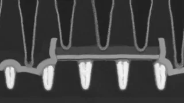
Two-dimensional materials, such as transition metal dichalcogenides (TMDs), have been under the spotlight for years because they enable transistors with channels only a few atoms thick, solving the electrostatic control issues that plague silicon at nanoscale dimensions. The main hurdle has always been bringing them to 300mm wafers with a reliable process and with both polarities — nMOS and pMOS — needed for low-power complementary logic. The team managed to integrate both transistor types with a contact pitch of 50nm, a milestone that brings 2D materials closer to mass production.
Density and efficiency: what changes for AI hardware
For those designing compute infrastructure, a 50nm pitch is not just a lab metric. A smaller pitch means more transistors per unit area, and with 2D materials this potentially translates into a drastic reduction in power dissipation at equivalent performance. In an era where AI models are ballooning and on-premise inference struggles to keep up with energy costs, a future generation of chips built on these transistors could reshape the TCO of local installations. This is not an imminent product, but a fundamental building block for architectures that, five or ten years from now, could make it viable to run large-scale LLMs on edge servers or corporate data centers without relying on centralized clouds.
Beyond silicon: a roadmap turning concrete
The semiconductor ecosystem is investing on multiple fronts simultaneously: gate-all-around transistors, 3D integration, new materials. The joint demonstration from imec, ASML, and TSMC marks a point of no return because it combines materials research, advanced lithography, and manufacturing scale. ASML contributes expertise in ultra-high-resolution exposure systems, TSMC its mastery of large-scale integration, and imec its role as a pre-competitive incubator. The fact that the result comes on a 300mm wafer rather than a lab fragment speaks volumes about the maturity achieved.
Outlook for on-premise deployment
Those evaluating on-premise deployments for AI workloads know that energy consumption and compute density are two sides of the same coin. The prospect of chips with 2D transistors capable of delivering more logic at the same thermal footprint could one day ease cooling constraints and make local hosting of increasingly large models practical. Of course, the path to commercialization is long and full of unknowns: material reliability, wafer-scale uniformity, integration with existing CMOS processes. But the signal from this collaboration is unmistakable: the post-silicon era is no longer science fiction, and the hardware that will power tomorrow’s AI is taking shape in today’s labs.


💬 Comments (0)
🔒 Log in or register to comment on articles.
No comments yet. Be the first to comment!