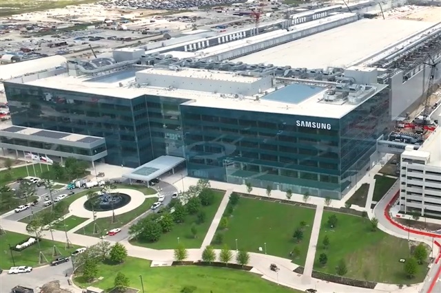
Samsung's semiconductor fab in Taylor, Texas, has reached a quiet but decisive milestone: the arrival of engineers from ASML, the Dutch company that holds a monopoly on extreme ultraviolet (EUV) lithography machines. The news, however sparse, carries enormous weight: it means the plant is ready to receive and activate EUV scanners, the multi-hundred-million-dollar technological jewels indispensable for producing chips below 7 nanometers.
Why ASML is the crossroads of the chip industry
Anyone following the chip industry knows that without ASML, there are no advanced processors. Its machines imprint patterns on silicon wafers with atomic precision, enabling transistor geometries otherwise unattainable. Samsung, like TSMC and Intel, depends on these tools to compete at the 5 nm, 3 nm, and beyond nodes. The arrival of technicians indicates that the Texas facility, after years of billion-dollar investments and delays, is moving toward operational status. The calibration and installation operations are handled directly by ASML personnel, a sign that the complexity of these devices demands ultra-specialized supervision.
A tangible impact on the AI supply chain
For those working with Large Language Models and on-premise infrastructure, this news has a strategic aftertaste. The chips manufactured in Taylor—likely Exynos SoCs and possibly chips for external customers—could include AI accelerators, GPUs, or NPUs designed for inference and training. In a scenario where NVIDIA GPUs remain expensive and hard to procure, every new manufacturing capacity on advanced nodes helps expand the potential supply, influencing the Total Cost of Ownership of local deployments. A fully operational Texas foundry could ease dependence on Asian suppliers, reducing the logistical and geopolitical risks dear to those managing sensitive deployments.
Technological sovereignty and the on-prem node
It is no coincidence that Samsung chose Texas. Proximity to large U.S. customers and the incentives of the CHIPS Act respond to a logic of shortening supply chains and technological sovereignty. For companies evaluating on-premise deployment, especially in regulated or air-gapped environments, the availability of hardware produced in North America reduces disruption risks and facilitates compliance with regulations like GDPR for locally processed data. AI-RADAR has already explored these trade-offs in its analytical frameworks for on-premise LLM, where the semiconductor supply chain is an often underestimated but critical factor for long-term planning.
The unknowns and the long-term potential
Of course, the road is still long. The Taylor fab has accumulated delays, and full activation will take more months. Moreover, the yield of advanced nodes is a typical unknown in early phases. But the signal is clear: the global manufacturing capacity for high-end chips is expanding, and this is positive news for anyone planning investments in self-hosted LLM platforms, where every watt and every dollar count. The arrival of ASML engineers is a technical nuance that only insiders fully grasp, but it tells a broader story: the slow, expensive, and geopolitically sensitive journey toward a chip production less concentrated in Taiwan. For our observatory, it means that on-premise solution providers should monitor the evolution of this fab, because when the first wafers come off the EUV line, the market might take notice sooner than expected.


💬 Comments (0)
🔒 Log in or register to comment on articles.
No comments yet. Be the first to comment!