Ask any hardware engineer why running inference on Large Language Models with Chinese chips is still a slow, costly, and inefficient operation, and the answer is almost always the same: it's not just about nanometers. There are three problems, openly referred to in Beijing's labs as 'the three walls': power dissipation, memory bandwidth, and interconnect scalability.
Domestically developed GPUs and accelerators — from Biren to Iluvatar Corex and training-oriented dies — have rapidly grown in raw compute power, but they remain hamstrung by a traditional memory system that can't keep pace. With models of 70 billion parameters and ever-widening context windows, the required VRAM explodes, and the latency of moving weights from memory to the compute die becomes the primary bottleneck. This is the memory wall: in conventional architectures, silicon wastes cycles and watts waiting for data.
The second wall is thermal. AI chips pushed to high frequencies to compensate for architectural limits generate power densities that demand liquid cooling or custom, expensive solutions, making deployment in standard on-premise datacenters difficult. The third, less visible but no less hard, is the interconnect wall: without access to NVLink or Infinity Fabric controlled by US companies, efficiently connecting hundreds of chips becomes a nearly prohibitive hardware-software co-design challenge.
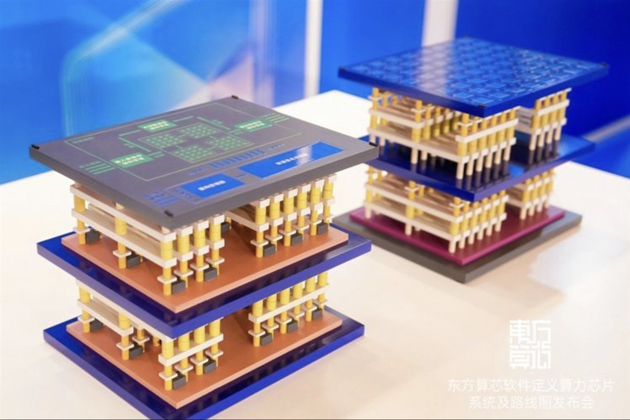
That is why Chinese manufacturers are taking a radical path: 3D memory. Not just HBM (High Bandwidth Memory) — access to which is anyway restricted by sanctions on Samsung and SK Hynix — but genuine vertical memory stacking architectures, with DRAM dies stacked directly on top of the logic processor, shortening data paths and multiplying available bandwidth per watt. The idea is to flip the problem: instead of chasing ever-finer manufacturing nodes, bypass the memory wall by increasing volumetric density.
While details on nodes and capacities remain closely guarded, the direction aligns with the needs of anyone wanting to run self-hosted LLM inference workloads. Without a bandwidth leap, the Total Cost of Ownership for keeping a mid-sized model on-premise becomes unsustainable, both in energy and in the number of accelerators required.
For those following AI-RADAR, this matters well beyond the lab: data sovereignty and the ability to keep models and inference out of US-based clouds depend on exactly these hardware choices. Chinese 3D memory chips are not a laboratory curiosity — they are the only path to building complete stacks — from silicon to runtime — that don't rely on Western-controlled licenses, patents, and supply chains. Whether this investment yields competitive chips will be decided by the fabs and advanced packaging plants still under construction, but the signal is clear: the next battle for on-premise AI will be fought over three-dimensional memory density, not just lithography.







💬 Comments (0)
🔒 Log in or register to comment on articles.
No comments yet. Be the first to comment!