L'Innovazione nel Processo Produttivo 18A
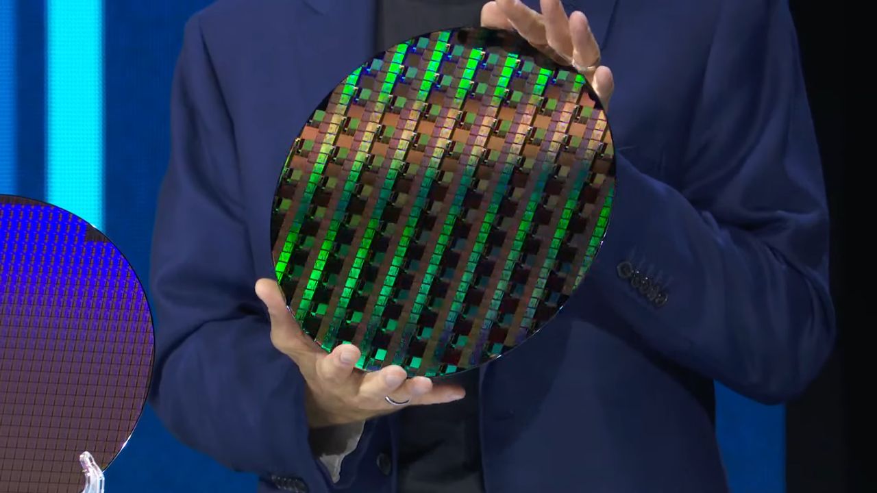
Intel sta dimostrando progressi significativi nel suo processo di produzione 18A, un nodo tecnicico cruciale per la prossima generazione di chip. Le recenti analisi di mercato evidenziano come l'azienda stia riuscendo a estrarre maggiore valore da ogni singolo wafer. Questo risultato è attribuibile a una strategia mirata all'ottimizzazione della resa, che include l'attenzione alle aree periferiche del wafer, tradizionalmente più complesse da gestire.
La riduzione della variabilità di resa su tutta la superficie del wafer è un fattore determinante. In passato, le imperfezioni o le deviazioni nelle specifiche potevano compromettere intere sezioni, riducendo il numero di chip funzionali. Migliorando l'uniformità del processo produttivo, Intel è in grado di convertire una percentuale maggiore di silicio grezzo in CPU vendibili, massimizzando così l'investimento in ogni ciclo di fabbricazione.
Dettagli Tecnici e Sfide di Produzione
Il nodo 18A rappresenta un balzo in avanti nella miniaturizzazione e nell'efficienza dei transistor. La produzione di chip a nodi così avanzati comporta sfide immense, dalla litografia EUV (Extreme Ultraviolet) alla gestione delle impurità a livello atomico. L'approccio di Intel, focalizzato sull'ottimizzazione dei bordi del wafer, suggerisce un affinamento delle tecniche di esposizione, deposizione e incisione che minimizzano i difetti anche nelle zone più esterne, dove le tolleranze sono spesso più difficili da mantenere.
Questo miglioramento nella resa non è solo una questione di quantità, ma anche di qualità. Una minore variabilità implica che i chip prodotti sono più consistenti in termini di performance e consumo energetico, aspetti fondamentali per i clienti enterprise. La capacità di produrre un numero maggiore di CPU affidabili da ogni wafer ha un impatto diretto sulla supply chain e sulla disponibilità di componenti critici per l'infrastruttura tecnicica globale.
Implicazioni per i Deployment On-Premise e il TCO
L'aumento della disponibilità di CPU avanzate, derivante da una migliore resa produttiva, ha ricadute significative per le organizzazioni che pianificano deployment on-premise. Una fornitura più stabile e prevedibile di hardware di ultima generazione consente ai CTO e agli architetti di infrastruttura di pianificare con maggiore certezza l'espansione dei propri data center, in particolare per carichi di lavoro intensivi come l'Inference e il training di Large Language Models (LLM).
Dal punto di vista del Total Cost of Ownership (TCO), una maggiore efficienza nella produzione di chip può tradursi in una migliore accessibilità dei componenti, influenzando i costi di acquisizione e, potenzialmente, riducendo i tempi di attesa per l'hardware. Questo è cruciale per le aziende che privilegiano la sovranità dei dati e il controllo diretto sull'infrastruttura, optando per soluzioni self-hosted o air-gapped. Per chi valuta deployment on-premise, AI-RADAR offre framework analitici su /llm-onpremise per valutare i trade-off tra costi, performance e controllo.
Prospettive Future nel Settore dei Semiconduttori
I progressi di Intel nel nodo 18A sottolineano l'intensità della competizione nel settore dei semiconduttori e l'importanza strategica dell'innovazione nei processi produttivi. La capacità di migliorare la resa dei wafer non solo rafforza la posizione competitiva dell'azienda, ma contribuisce anche a soddisfare la crescente domanda globale di potenza di calcolo.
Mentre l'industria continua a spingere i limiti della legge di Moore, l'attenzione alla micro-ottimizzazione di ogni fase del processo produttivo diventerà sempre più critica. Questi sviluppi non solo garantiscono una maggiore efficienza economica per i produttori, ma assicurano anche che l'ecosistema tecnicico globale possa contare su un flusso costante di componenti sempre più performanti e affidabili, essenziali per l'avanzamento dell'intelligenza artificiale e di altre tecnicie emergenti.


💬 Commenti (0)
🔒 Accedi o registrati per commentare gli articoli.
Nessun commento ancora. Sii il primo a commentare!