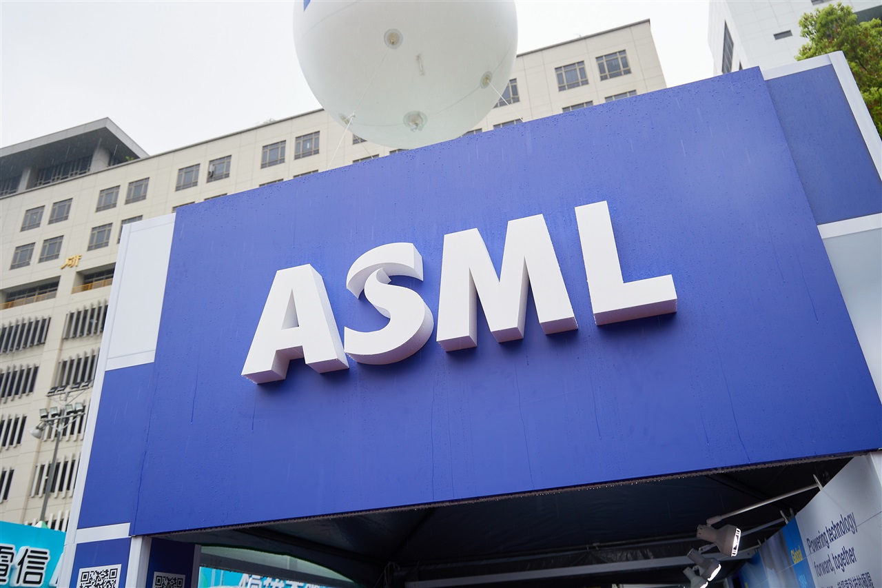
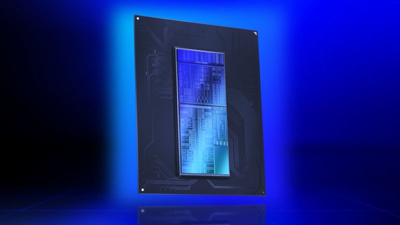
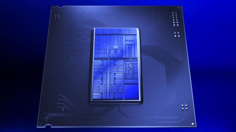
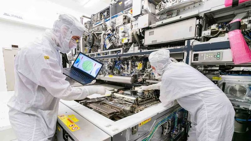
Intel has reached a long-awaited milestone: the qualification of High-NA EUV lithography for its Panther Lake processors. News emerging from the supply chain signals that the first chips built with ASML's next-generation scanners are now ready for high-volume manufacturing. Meanwhile, ASML is accelerating the technology transfer to TSMC and Samsung, the two foundry giants that produce silicon for Nvidia, AMD, Qualcomm, and much of the AI ecosystem.
High-NA EUV increases the numerical aperture from 0.33 to 0.55, enabling feature printing at a roughly 8-nanometer pitch. This is not a mere incremental step: it drastically reduces the need for multi-patterning, which in previous generations stretched process times, increased defectivity, and squeezed yields. Fewer masks, fewer lithography passes, more functioning transistors per wafer. On the cost side, the benefit unfolds over the maturity curve: early lots bear the huge capital expenditure (each High-NA tool costs over 300 million euros), but once running at steady state, the lower complexity can stabilize or even lower the cost per transistor, easing one of the strongest pressures that have slowed advanced-node progress.
For those focused on on-premise deployment of Large Language Models, the transition carries structural weight. Logic chips built with High-NA—initially CPUs, but quickly followed by GPUs and dedicated accelerators—will deliver higher compute density within the same thermal envelope. Translation: more tokens per second per watt, and the ability to run models with extended context windows without resorting to prohibitive multi-GPU setups. In a landscape where data sovereignty pushes enterprises and institutions to keep inference inside their own data centers, more efficient silicon narrows the gap with cloud offerings and strengthens the economic case for self-hosted infrastructure.
A second-order consequence is less obvious. High-NA EUV does not just shrink transistors; it changes how chips are designed. The finer resolution allows memory and logic blocks to be integrated with relaxed constraints, opening the door to microarchitectures that favor inference throughput without sacrificing programmability. Design teams at Nvidia, AMD, and hyperscalers developing in-house ASICs (Google, Amazon, Microsoft) can exploit these more flexible design rules to optimize layouts around transformer workloads, rather than bending to inherited lithographic limits. It is no coincidence that TSMC and Samsung are already setting up pilot lines: whoever arrives first with a mature High-NA process sets the rules for the next generation of AI accelerators.
Intel, for its part, has every incentive to capitalize on the time advantage. Panther Lake, expected in the second half of the decade, will be the first consumer product to use High-NA, but Intel Foundry Services is already in talks with external customers eager to bring their designs onto that node. If the company can demonstrate competitive yields, it could threaten the TSMC-Samsung duopoly just as demand for AI chips explodes—an outcome that would redraw the geography of advanced manufacturing and, with it, the supply chain for organizations building on-premise AI infrastructure.



💬 Comments (0)
🔒 Log in or register to comment on articles.
No comments yet. Be the first to comment!