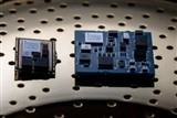
JCET is pouring $1.1 billion into a production expansion that isn't about transistor fabrication but about the next step: advanced packaging. The news, reported by Reuters, signals a shift in direction for China's semiconductor industry, increasingly constrained by export restrictions on cutting-edge technology. While media attention remains fixed on 3-nanometer nodes, the decisive game for artificial intelligence is being played on a less flashy but equally strategic field: how to assemble multiple chips, high-bandwidth memory (HBM), and interconnect systems without losing performance or driving up power consumption.
The heart of AI is not just silicon
For some time now, the performance of Large Language Models has not depended solely on transistor density. With Moore's Law slowing, the industry has shifted its center of gravity toward packaging: techniques like TSMC's CoWoS (Chip on Wafer on Substrate) or Intel's EMIB make it possible to bring memory closer to the processor, multiply bandwidth, and handle the massive data volumes that inference and training demand. Without advanced packaging, even the most powerful chip would be hobbled by bottlenecks in communication with VRAM. For those evaluating on-premise deployments, these technologies have a direct impact: they determine the actual availability of accelerators, energy consumption, and total cost of ownership (TCO).
JCET's investment – the Chinese company specializes in packaging and testing – shows how Beijing is trying to circumvent sanctions that limit access to advanced manufacturing nodes. Unable to compete on lithography, China is strengthening its position in chiplet assembly and the integration of diverse components, an approach that would still allow it to build complex systems for AI. It's a familiar strategy: Chinese AI firms are stockpiling NVIDIA's A800-series GPUs, but true autonomy comes from the ability to package their own accelerators in-house, perhaps by combining modules produced with less sophisticated technologies.
A supply chain under strain
The $1.1 billion expansion comes at a time of heavy global demand for advanced packaging. TSMC, the sector leader, is struggling to keep up with CoWoS orders, and lead times are lengthening, holding back the availability of new AI hardware. In this scenario, a strengthened JCET could become a second-tier supplier for Chinese chipmakers, unlocking production capacity for the local market and, indirectly, influencing global prices and volumes. For on-premise environments – where organizations seek to retain control over data and latency – supply chain diversification is a critical variable: having multiple sources of accelerators reduces the risk of dependence on a single vendor.
Geopolitics and technological sovereignty
JCET's move is not just industrial. It signals the extension of the technological competition between the United States and China to a new link in the value chain. American sanctions have so far focused on lithography equipment and high-performance GPU design, but advanced packaging could become the next front. For European companies evaluating self-hosted AI infrastructure, these tensions translate into uncertainty about the future availability of key components. It is no coincidence that AI-RADAR closely follows hardware market developments: deployment choices – cloud, hybrid, or on-premise – are increasingly tied to the robustness of supply chains and the ability to plan for the long term.
In short, JCET's investment is not just a number. It is an indicator of how the global industry is redrawing the maps of computing power, shifting the balance from the single transistor to the complexity of integration. Anyone planning an AI data center today would do well to look not only at the GPU spec sheet, but also at who puts it together and how.


💬 Comments (0)
🔒 Log in or register to comment on articles.
No comments yet. Be the first to comment!