AI Redefines Semiconductor Testing
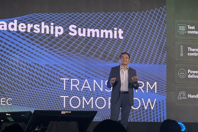
Artificial intelligence is permeating every aspect of the technology industry, and the semiconductor sector is no exception. A key observation comes from the CEO of AEM, who recently highlighted how AI is revolutionizing semiconductor testing. This statement underscores a crucial trend: the adoption of AI-driven methodologies to address the increasing complexity of modern chips, particularly those designed for AI workloads.
Semiconductor manufacturing is an inherently complex process where precision and reliability are non-negotiable parameters. With technological advancements, chips are becoming denser and more multifunctional, rendering traditional testing methods less efficient or even insufficient. The integration of AI promises to overcome these limitations, introducing a new paradigm for quality and performance verification.
The Impact of AI on Testing Processes
The application of artificial intelligence in semiconductor testing manifests in several areas. One of the most evident is the automation of visual inspection, where computer vision algorithms can identify microscopic defects with superior speed and accuracy compared to human inspection. This not only accelerates the process but also reduces the potential for errors, ensuring greater uniformity in product quality.
Furthermore, AI can optimize test pattern generation and verification sequences. Machine Learning models are capable of analyzing vast amounts of historical test data to predict potential failure points, identify hidden correlations, and generate more targeted and effective tests. This predictive approach allows for a reduction in overall test time and an improvement in defect coverage, a fundamental aspect for high-performance chips like GPUs and AI accelerators, which demand impeccable accuracy for their complex inference and training operations.
Implications for Infrastructure and Deployment
The adoption of AI in semiconductor testing entails significant infrastructure requirements. Running Machine Learning models for test data analysis, pattern optimization, or visual inspection demands considerable computational power, often relying on GPUs with high VRAM and throughput. For companies in this sector, the decision between on-premise deployment and cloud solutions becomes crucial.
Testing in production environments, where latency is a critical factor and data is extremely sensitive (proprietary designs, manufacturing processes), often favors a self-hosted approach. An on-premise deployment ensures direct control over hardware, data sovereignty, and the ability to operate in air-gapped environments to maximize security. Although the initial investment (CapEx) might be higher, a long-term TCO (Total Cost of Ownership) analysis can reveal significant advantages, especially for constant and predictable workloads. For those evaluating on-premise deployment, AI-RADAR offers analytical frameworks on /llm-onpremise to assess specific trade-offs related to performance, costs, and security.
Future Perspectives and Challenges
The AI-driven transformation of semiconductor testing is an ongoing process. Challenges include the need for high-quality training datasets, the integration of AI systems with existing test equipment, and the training of personnel with hybrid skills in semiconductor engineering and artificial intelligence. However, the potential benefits are enormous: faster development cycles, reduced testing costs, and, most importantly, enhanced reliability for the components that power the entire digital economy.
The AEM CEO's statement underscores a clear direction for the industry: AI is no longer just a tool for data processing but a fundamental element for ensuring quality and innovation in critical hardware manufacturing. Companies that invest in robust infrastructure and advanced AI methodologies will be at the forefront of shaping the future of silicio.


💬 Comments (0)
🔒 Log in or register to comment on articles.
No comments yet. Be the first to comment!