The Race for Advanced Packaging: A Strategic Factor for AI
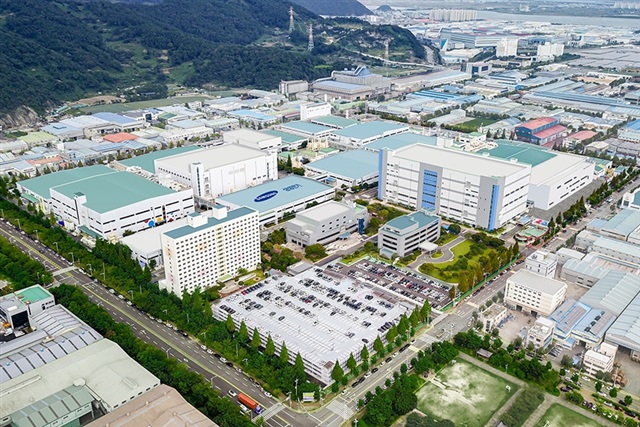
South Korea has launched an accelerated strategy to close the technological gap in advanced chip packaging, an increasingly critical sector within the semiconductor industry. This initiative sees the country directly competing with established leaders like Taiwan and the growing influence of China. Companies such as Samsung Electro-Mechanics are at the forefront of these efforts, aiming to strengthen Korea's position in a phase of chip production that significantly determines the final performance of components.
Chip packaging, often underestimated compared to wafer fabrication, has become a fundamental bottleneck for the performance of modern processors, especially those intended for artificial intelligence workloads. It is no longer just about protecting the silicon die, but about integrating multiple components into a single module, optimizing communication and efficiency.
The Crucial Role of Advanced Packaging for LLMs
For Large Language Models (LLM), advanced packaging is a distinguishing element that directly influences training and Inference capabilities. Technologies like High Bandwidth Memory (HBM), which vertically stacks multiple DRAM dies, are made possible by sophisticated packaging techniques. This approach dramatically increases memory bandwidth (VRAM), a critical factor for powering AI models that require rapid access to enormous amounts of data.
Efficient packaging reduces distances between components, minimizing latency and power consumption. This translates into more powerful and performant GPUs, capable of handling larger batch sizes and processing a higher number of Tokens per second, vital aspects for those operating with large-scale LLMs. The ability to compactly and efficiently integrate CPUs, GPUs, and memory within a single package is key to unlocking new frontiers in computational efficiency.
Implications for On-Premise Deployment and Data Sovereignty
Advancements in chip packaging have direct implications for organizations evaluating LLM deployment in self-hosted or air-gapped environments. GPUs with advanced packaging offer greater compute density and better energy efficiency, factors that significantly impact the Total Cost of Ownership (TCO) of an on-premise infrastructure. Lower power consumption and reduced cooling requirements can offset the initial investment in high-end hardware.
Furthermore, a country's ability to control the entire semiconductor production pipeline, from design to fabrication to packaging, is fundamental for data sovereignty and supply chain security. For companies operating in regulated sectors or with stringent compliance requirements, access to hardware produced in diversified or controlled geographical contexts can be a strategic advantage. AI-RADAR offers analytical frameworks on /llm-onpremise to evaluate the trade-offs between performance, TCO, and sovereignty requirements for on-premise deployments.
Future Prospects and Global Competition
Competition in advanced packaging is set to intensify, with massive investments in research and development from all major players. Success in this field will not only secure significant market share but also strengthen the resilience of global supply chains, reducing dependence on a single production hub.
For companies developing and implementing AI solutions, the evolution of packaging will translate into a wider choice of optimized hardware, with ever-increasing performance and improved energy efficiency. This technological race is a clear indicator of how innovation at the silicon and packaging level is intrinsically linked to the future of artificial intelligence and its practical implementation in enterprise contexts.


💬 Comments (0)
🔒 Log in or register to comment on articles.
No comments yet. Be the first to comment!