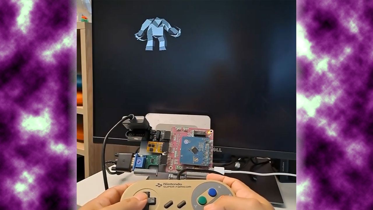
A 240,000-transistor chip is enough to bring into focus a shift that many in the data center world pretend not to see. The TinyGPU v2.0, which has now passed real-world tests, doesn’t aim to compete with an H100: it delivers 3D graphics at 15 frames per second, and version 3.0 is already slated for 2026. This news, read through the lens of those designing on-premise architectures and edge infrastructures, weighs more than the spec sheet reveals.
Miniaturization of graphics chips isn’t new, but the arrival on tested, functioning silicon lights up a clear signal: the pendulum of computing power is beginning to swing away from cloud giants toward devices we control directly. This isn’t about frame rate: 15 FPS is enough for industrial interfaces, interactive signage, biomedical control panels, or IoT applications where latency to a remote server is unacceptable. In these contexts, every watt saved and every byte of data that never leaves the device becomes strategic currency.
Why such a small chip scares centralized giants
The real stake is computational sovereignty. When an organization can handle the entire graphics or inference workload on a fingernail-sized device, reliance on external infrastructure — with its transmission costs, delays, and compliance risks — becomes optional. It’s not science fiction: the TinyGPU v2.0 tests suggest that entire production processes could be re-engineered around self-contained silicon, without a permanent cloud connection.
Who wins and who loses? Designers of embedded devices and industrial solutions gain a new hardware building block to lock down their data and reduce TCO by eliminating recurring subscription flows. Cloud service providers, on the other hand, see erosion of a user base that until now delegated even the most basic rendering or simple inference tasks to them, because no economically viable local alternative existed.
It’s important not to mistake the TinyGPU v2.0 for an LLM accelerator: with this transistor density, even a quantized language model wouldn’t fit. Yet the technological direction shows that if 240,000 transistors suffice for 3D, integrating dedicated AI accelerators on similar dies — with on-chip memories and negligible power draw — is a path now wide open. This is exactly the scenario AI-RADAR tracks for those evaluating on-premise deployment: you don’t need an H100 to run inference on a vertical model with a few billion parameters, and often a hybrid edge approach can slash operational bills without sacrificing usable performance.
The fact that a version 3.0 is already on the roadmap for 2026 confirms that this isn’t an academic experiment but a concrete race toward ever more compact silicon capable of reshaping the hierarchies of distributed computing. What’s at stake isn’t just data, but control over it — and who pays to process it.






💬 Comments (0)
🔒 Log in or register to comment on articles.
No comments yet. Be the first to comment!