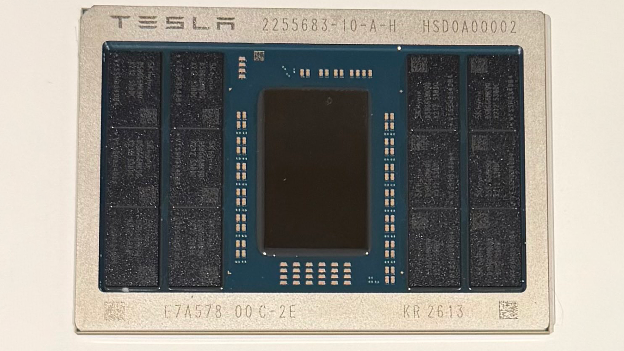
The news lands like a thunderbolt in an industry where every nanometer counts: Tesla has taped out its AI5 chip at Samsung Foundry on a 2nm-class process, and production is now imminent. The milestone comes months after a similar achievement with TSMC, confirming the company’s push to diversify sources for the computational heart of its fleet.
This is not just a supply-chain story. AI5 is the next processor bound for Tesla vehicles to run autonomous driving workloads – a blend of complex neural network inference, multi-camera video streams, and real-time decision-making with near-zero latency requirements. All of it must happen onboard, within tight thermal and power envelopes, without leaning on remote data centers. In other words, it’s the ultimate acid test for extreme edge deployment: each car is an isolated compute node where sensor data stays local and is processed on the spot, with powerful implications for data sovereignty and operational resilience.
Why Samsung now counts as much as TSMC
Pairing Samsung alongside TSMC for a bleeding-edge 2nm-class node is no trivial choice. For years, the Korean foundry chased its Taiwanese rival in yield maturity and manufacturing prowess. Securing a tape-out on a “2nm-class” process – most likely featuring Gate-All-Around (GAA) transistors, which Samsung introduced ahead of others – suggests that the densest nodes are no longer the monopoly of a single player. The structural effect is clear: it lowers the choke-point risk for companies like Tesla, which design custom ASICs for specific AI loads and cannot afford single-supplier dependency.
For the community tracking on-premise LLM deployments and inference, the development is instructive. The density and energy efficiency of a 2nm node allow larger models (parameter counts in the tens of billions) to run without blowing the thermal budget of an embedded platform. If an electric vehicle can afford to run a transformer in real time, the same principle applies to on-prem servers, industrial edge gateways, and air-gapped scenarios where energy cost and physical space are tight constraints. You don’t need to be Tesla to benefit from advanced node maturation; Tesla is simply showing what happens when you push the envelope.
Less latency, more sovereignty
AI-RADAR’s interest in stories like this lies in the subtext: when a processor rides a 2nm-class process and is designed for inference directly at the data collection point, the classic compromises between compute power and privacy disappear. It’s no longer a choice between streaming video feeds to the cloud or settling for stripped-down models – the silicon sustains workloads that, until yesterday, were unthinkable outside a rack. For companies evaluating on-prem deployment of language or vision models, this is a signal not to ignore: the enabling hardware is coming even beyond the usual circle of GPU suppliers.
The dual TSMC–Samsung strategy also affects TCO calculations. Putting two foundries in competition on a project of this scale can moderate chip manufacturing costs, and with them the per-unit cost of the final system. Although Tesla does not sell its processors to third parties, the ripple effect through the supply chain will be felt, encouraging other AI chip designers to consider multi-foundry options for leading-edge nodes.
We lack numerical specifications – the Austin-based company is notoriously tight-lipped with figures – but the very fact that a 2nm tape-out is labeled “production-starting-soon” suggests the risk-production phase has been cleared. If timelines hold, the first AI5 units could be on the road within a 12–18-month window. Long enough to reshape the boundaries of what we call edge computing.




💬 Comments (0)
🔒 Log in or register to comment on articles.
No comments yet. Be the first to comment!