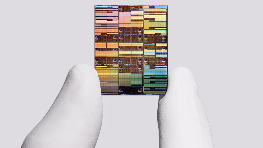
IBM has stirred the microelectronics world by claiming it has built the first sub-1nm transistor technology, at what it calls the 0.7 nm – or 7-angstrom – node. The announcement, reported by The Next Web, lands at a moment when the semiconductor industry has been straining toward that symbolic barrier for years, but also knows that process node names no longer tell a straightforward physical story. The news deserves a careful reading from anyone who tracks the hardware that will eventually power on-premise AI.
Crossing into the angstrom era
For decades the nanometer served as the yardstick of transistor progress. Dropping below 1 nm pushes us into the realm of angstroms (10 Å = 1 nm), where quantum effects can no longer be ignored. IBM, a long-time player in basic semiconductor research, presents this architecture as a proof point of how far materials and gate geometries can be pushed. The company has not disclosed lithographic process details or manufacturing partners, but the mere claim of a working 7 Å transistor is enough to rattle the sector.
Why “0.7 nm” is not a physical measurement
Process node names ceased to correspond to actual gate lengths years ago. Labels like “5 nm” or “3 nm” are marketing tags that signify a generational leap in density and performance, not a physical dimension. The same holds for 0.7 nm: it does not mean each transistor is seven tenths of a nanometer wide, but that the technological step promises a jump in energy efficiency and in the number of transistors packed into a square millimeter. IBM itself knows this game well, having contributed to breakthroughs such as Gate-All-Around (GAA) transistors and nanosheet architectures, often previewed in labs long before reaching commercial products.
What it means for on-premise hardware
For those designing self-hosted compute infrastructure – say, LLM inference clusters or fine-tuning servers – every advance in transistor density translates, on paper, into a double promise: lower power consumption at a given workload and higher compute capacity within the same physical footprint. In on-premise scenarios, where space, cooling, and TCO constraints are tight, chips built on more advanced processes can tip the balance over the medium term. However, the gap between a lab demonstrator and a buyable product often stretches to five years or more, and the road to mass production at 7 Å is littered with engineering and economic hurdles.
The lesson of past nodes
Recent history shows that grand node announcements do not always turn into real availability. Technologies such as strained silicon, high-k metal gate, or FinFET took years to become mainstream, and only when foundries (TSMC, Samsung, Intel) embedded them into their roadmaps. IBM, which sold its manufacturing division to GlobalFoundries in 2015, is today primarily a research center that licenses its discoveries. Whether the sub-1nm node reaches the market therefore depends on who picks up the baton and with what investments. For deployment decision-makers, caution remains the watchword: spec sheets will matter more than press releases.
Beyond a single transistor: impact on AI accelerators
The next step, once the node is mastered, is to carry it into specialized accelerators – GPUs, TPUs, inference ASICs – where efficiency per token processed and throughput become key metrics. In on-premise LLM deployments, reducing watts per inference lowers operational costs and makes it economically viable to keep data in-house, meeting sovereignty and compliance needs. IBM did not mention AI applications in its announcement, but the entire semiconductor supply chain is increasingly shaped by artificial intelligence workloads. That means every step toward denser, more efficient transistors directly concerns those building their own hardware stack.
A roadmap yet to be written
IBM’s announcement should be read as a directional signal, not as an imminent product. The industry still has intermediate nodes – 2 nm, 1.4 nm – to navigate before anything commercially available falls below the 1 nm mark. And even then, one will need to verify how much the lab gains translate into real-world performance-per-watt and TCO improvements in production environments. AI-RADAR will keep tracking process technology advances because every lithography breakthrough redraws the boundaries of what is possible for large-scale on-premise computing.


💬 Comments (0)
🔒 Log in or register to comment on articles.
No comments yet. Be the first to comment!