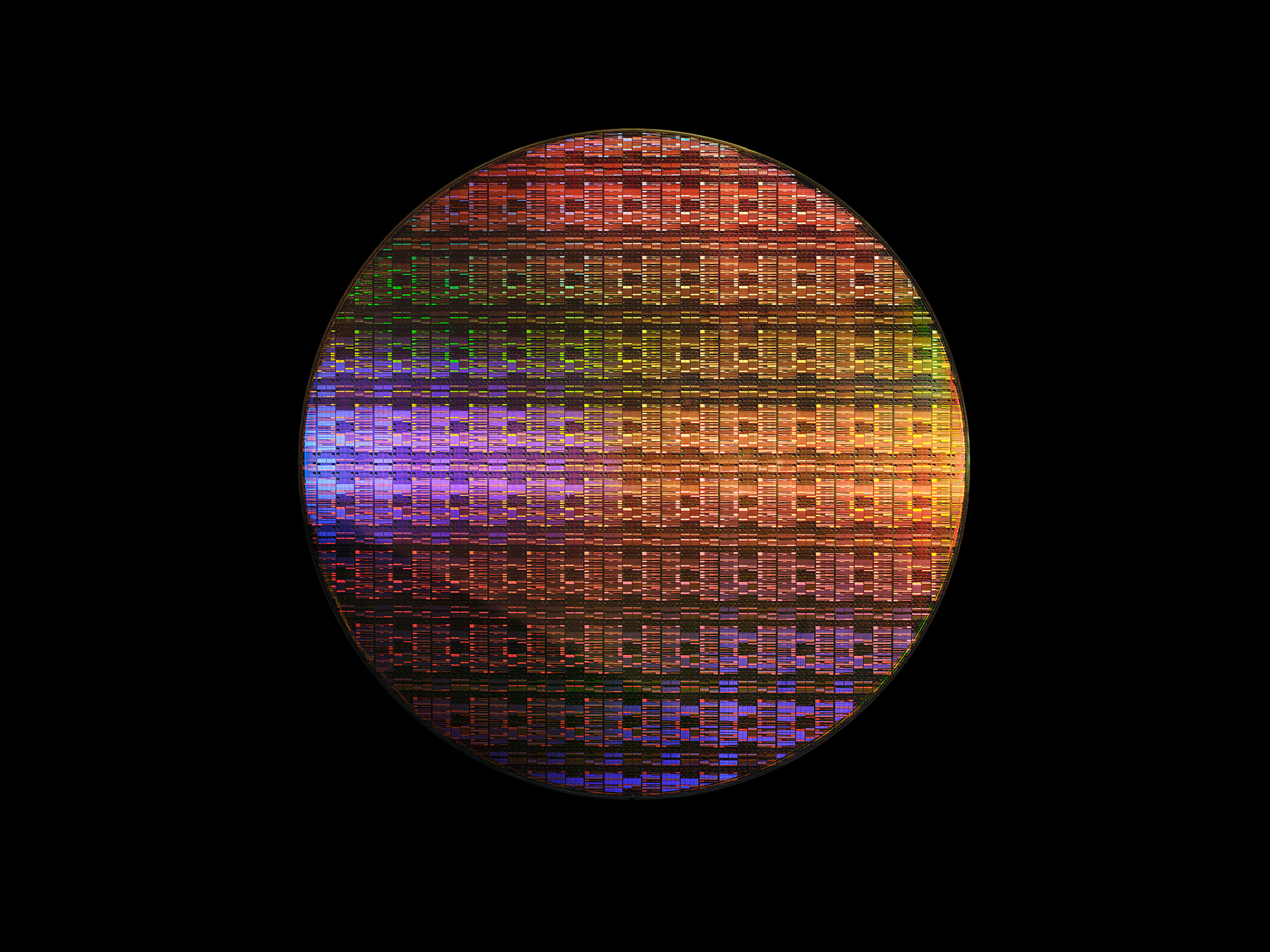
If until yesterday miniaturization meant shrinking the feature size, as of roughly today it also means stacking. IBM has unveiled its nanostack transistor architecture, a roadmap aimed squarely at the sub-1nm era expected in the 2030s. It’s not a simple restyling of FinFET or gate-all-around, but an injection of the third dimension: wafer stacking to build taller chips, and only in this way, denser ones.
The end of the planar chase
For decades the semiconductor industry has chased Moore’s Law by pushing lithography toward ever finer geometries. Down near the nanometer, however, quantum effects and thermal dissipation have turned every step into a balancing act. With nanostack, IBM changes strategy: instead of continuing to dig into the plane, it builds vertically. The approach involves stacking transistor layers on multiple levels, increasing logic density without necessarily squeezing lateral dimensions further.
The timing is indicative: the horizon is 2030 and beyond, a period when sub-nanometer nodes will demand radically new materials and architectures. Stacking itself is not new — 3D NAND memories and advanced packaging already use it — but bringing it to logic transistor scale in high volume is a different game.
Density for on-premise inference
For those evaluating AI deployments away from the cloud, transistor density is no academic exercise. Denser chips, for a given area, offer more cores, more SRAM, more accelerators: resources that translate into larger context windows, lower inference latency, and the ability to run LLM models entirely locally without saturating the data center’s thermal budget. If nanostack delivers, the hardware arriving in the racks of the next decade could execute workloads unthinkable today without surrendering data to external services.
Data sovereignty, after all, is not purchased with policies alone: it is built with silicon. Every density jump reduces the cost per token processed on-premise and pushes out the threshold beyond which surrendering to the cloud becomes tempting. IBM isn’t yet discussing power or process specifics, but the very idea of stacking logic layers opens the door to a potentially more favorable TCO for those managing bare-metal infrastructure.
The manufacturing complexity knot
3D architectures also bring new problems. Heat trapped between layers, alignment tolerances, wafer yield: every stacking step increases fabrication complexity and, in the near term, cost. IBM’s research will aim to untie these knots before the technology becomes commercial. Meanwhile, the message is clear: the end of planar miniaturization is not the end of performance growth. It’s just the beginning of a phase where how you put the bricks together matters more and more, not just how small they are.
For those tracking on-premise deployment evolution, the lesson is stark. Infrastructure choices made today with current GPUs and accelerators will need revisiting when vertical architectures enter servers. Software elasticity — containerization, serving frameworks, orchestration — will have to cope with hardware that distributes heat and memory in unprecedented ways. AI-RADAR follows these developments closely, because the next chip generation won’t just be smaller: it will be stratified, literally.


💬 Comments (0)
🔒 Log in or register to comment on articles.
No comments yet. Be the first to comment!