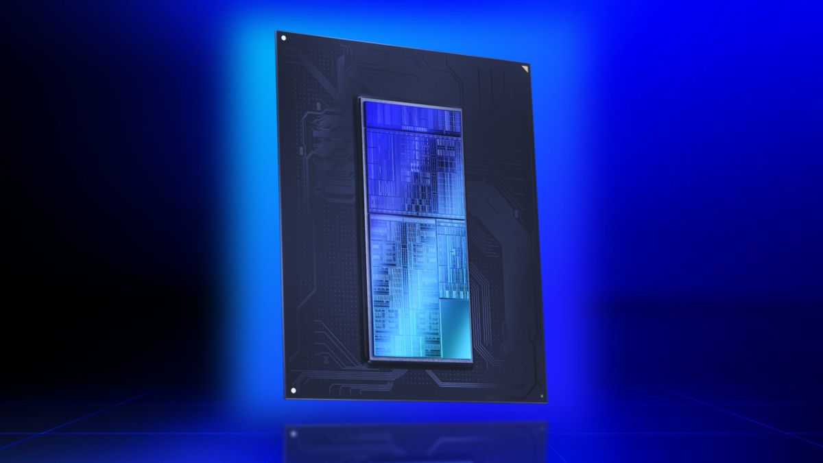
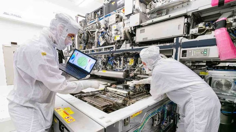
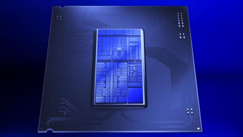
With a move that marks a turning point in the semiconductor race for AI, Intel has confirmed that it is the first manufacturer in the world to use ASML's High NA EUV scanners for high-volume production of logic chips. The first examples concern specific layers of the upcoming Panther Lake processors, built on the 18A node, now qualified for 0.55 numerical aperture lithography.
High NA EUV (extreme ultraviolet) increases the numerical aperture from 0.33 to 0.55, enabling the projection of finer patterns onto silicon and thus reducing the minimum feature size. In practice, this means smaller and more energy-efficient transistors—two critical parameters for AI workloads that push data centers to thermal and power limits.
For those running on-premise infrastructure, this is not just an industry insider update. Intel's ability to bring this lithography into volume production paves the way for server processors and accelerators that can perform LLM inference at lower power consumption per token. In a context where the TCO of self-hosted solutions heavily depends on energy costs and compute density, such a technological leap translates into lower operational expenses and greater sustainability.
The on-premise loop tightens
The arrival of more performant chips on identical power envelopes has a ripple effect. First, it reduces dependency on the cloud for sensitive workloads: if local hardware can compete in latency and throughput, enterprises managing regulated data or pursuing digital sovereignty have fewer reasons to outsource processing. Second, edge AI benefits directly from more frugal silicon, as thermal and power constraints are strict.
Intel is not alone in this game, but its lead in mass production with High NA EUV signals renewed competitiveness for its foundry, potentially accelerating the entire ecosystem. Other AI chip designers, from GPU vendors to specialized ASIC creators, could tap Intel’s 18A node to bring even more tailored on-premise solutions to market. Competition benefits everyone: shorter development timelines and more hardware options for those setting up in-house inference clusters.
Of course, the transition won't be immediate: Panther Lake chips on 18A are expected in the coming years, and high-volume manufacturing with this technology will need to overcome the usual yield and scalability challenges. Still, the message is unequivocal. The semiconductor supply chain's industrial plan is squarely aimed at delivering ever denser and more efficient silicon, precisely as demand for local inference and distributed training grows. For IT decision-makers evaluating on-premise architectures for their LLMs today, this is confirmation that hardware innovation pace is strong and that self-hosted solutions will become increasingly competitive in the coming refresh cycles.





💬 Comments (0)
🔒 Log in or register to comment on articles.
No comments yet. Be the first to comment!