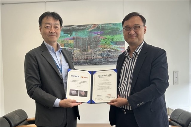
The news comes from JNTC-TOPPAN, a Korean-Japanese joint venture that is accelerating the development of glass substrates for advanced semiconductor packaging. It’s not a niche technical detail but a signal of how the industry is rethinking the physical foundations of the hardware that runs the most demanding Large Language Models. For anyone tracking on-premise deployments, the question has long been: how much further can board efficiency scale without changing the base materials?
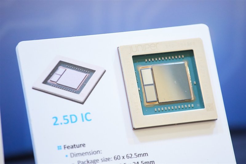
Today’s multi-chip packaging (GPU with HBM memory, interposer, substrate) is dominated by organic solutions, typically based on epoxy resins and fiberglass. But as the number of chiplets grows and power dissipation climbs, the thermal expansion coefficient of these materials diverges more and more from that of silicon. The result is mechanical stress that caps achievable dimensions and interconnect density. Glass, with a thermal expansion much closer to silicon’s, promises to loosen this constraint, paving the way for larger interposers, finer lines, and ultimately more transistors and memory lanes per package.
The JNTC-TOPPAN initiative is interesting not only for the technology itself but for the industrial geography it represents. JNTC comes from the display glass world, Toppan from electronic packaging materials. Their collaboration signals that the substrate supply chain is pulling skills from a variety of sectors just as foundries and chip designers (from NVIDIA to AMD, and Intel) push for ever more complex packages. The ensuing question is who will control the cost and availability of these critical substrates, because the shift to glass could concentrate production in the hands of a few players capable of handling ultrathin sheets at scale, with repercussions on pricing and supply that reach all the way to the on-premise data center.
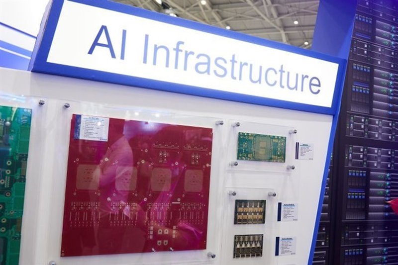
For the enterprise user evaluating a self-hosted inference cluster, the technical trajectory has concrete meaning. If a single accelerator can host more memory and increase effective bandwidth without changing the lithography node, the space, power, and cooling requirements for running a 70-billion-parameter model with INT8 or FP16 quantization may drop. What today takes four cards could tomorrow run on two, reducing Total Cost of Ownership and simplifying operations. This is not a point prediction but a structural vector that shifts the break-even point between cloud and local hardware for a growing number of workloads.
To be sure, the road to mass production is not obstacle-free: handling ultrathin glass sheets demands entirely new processes compared with organic substrates, and initial yields may not be competitive. Yet the mere fact that a consortium with a background in glass and packaging is investing signals that major AI chip buyers see a performance wall looming with current materials. It’s a cue for those designing the next generation of on-premise infrastructure: packaging constraints are as decisive as the manufacturing node, and whoever removes them first can redraw the power hierarchy at a given cost.




💬 Comments (0)
🔒 Log in or register to comment on articles.
No comments yet. Be the first to comment!