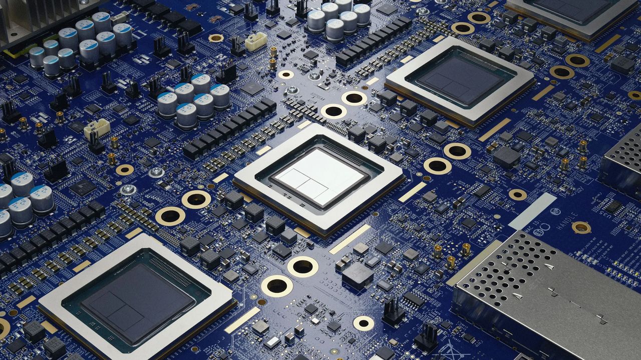
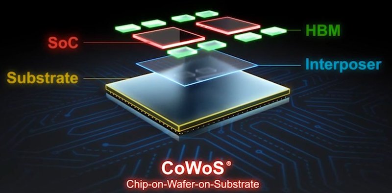
The news that Google has turned to Intel for advanced packaging of its 9th-generation TPUs is more than a contract. It is a quiet earthquake in the semiconductor supply chain, a vote of confidence in Intel's Embedded Multi-die Interconnect Bridge (EMIB) that cracks TSMC's near-uncontested dominance and its CoWoS (Chip-on-Wafer-on-Substrate) technology. For years, anyone wanting to push AI chip performance beyond monolithic limits — GPUs, accelerators, ASICs — had to reckon with CoWoS bottlenecks, whose production capacity became a structural chokepoint. Intel, with EMIB, offers a second path.
EMIB is not new: Intel already uses it in products like the Sapphire Rapids data center processors and some FPGAs. The technology replaces CoWoS's silicon interposer with a small bridge embedded in the organic substrate, connecting chiplets at ultra-high density without passing through an expensive intermediate silicon wafer. The result is greater design flexibility and, at least on paper, lower costs. But the market had been cautious: relying on Intel Foundry Services meant betting on a still-building reality with roadmaps yet to be proven.
Google's reported choice — sourced by multiple outlets and not denied — changes the game. For 9th-gen TPUs, designed for inference and training of large models, interconnect density and thermal management are critical. That Mountain View's team judged EMIB comparable or superior to CoWoS sends a strong signal to the entire ecosystem.
What it means for the on-premise AI ecosystem
AI-RADAR readers know that packaging technology is not an esoteric detail: it directly affects the availability and cost of accelerators powering on-premise clusters. Today, those building self-hosted AI infrastructure face a market where demand for advanced chips outstrips supply and CoWoS constraints impact delivery times and final prices. A viable alternative to TSMC, even for part of production, can mean fewer bottlenecks, stronger negotiating power, and, over time, a lower Total Cost of Ownership (TCO).
EMIB also aligns with the chiplet philosophy, enabling hybrid architectures where compute, HBM memory, and I/O can be optimized separately. For on-premise LLM deployments — where VRAM is often the real limit — this modularity could lead to more granular, upgradeable solutions without redesigning the entire silicon. Intel is also pushing the UCIe (Universal Chiplet Interconnect Express) standard to create an open ecosystem of interoperable chiplets, breaking vendor walled gardens.
Of course, the road is long. Intel Foundry must prove it can scale EMIB with high yields and competitive costs at volumes comparable to TSMC. And TSMC is not idle: it is aggressively expanding CoWoS capacity and has announced hybrid variants. But diversification is now a geopolitical and industrial necessity. For those evaluating a local AI deployment — where supply chain control is integral to data sovereignty — having multiple advanced packaging suppliers reduces the risk of dependency on a single production node, often concentrated in geopolitically sensitive areas.
The Google news thus signals a turning point: the AI chip market is becoming bipolar in packaging. And for on-premise infrastructure planners, it means more options, potentially shorter lead times, and a more distributed manufacturing geography. It is not yet a revolution, but it is the first brick in a wall that will no longer see TSMC as the sole gatekeeper.



💬 Comments (0)
🔒 Log in or register to comment on articles.
No comments yet. Be the first to comment!