Lam Research's Innovation in Panel Level Packaging
Lam Research, a key player in the semiconductor manufacturing equipment sector, is focusing its efforts on advancing Panel Level Packaging (PLP) through its Salzburg center. This initiative signals a clear push towards optimizing panel production processes, a critical area for the evolution of modern electronics.
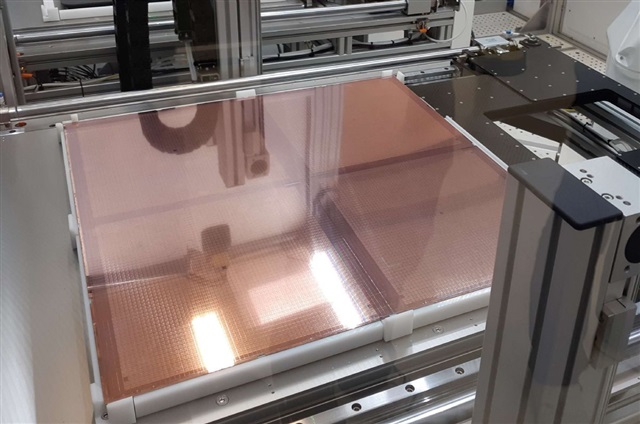
PLP represents an advanced packaging technique that aims to improve efficiency and reduce costs in chip manufacturing. Unlike traditional methods that process chips on circular wafers, PLP uses rectangular, panel-shaped substrates, allowing for the production of a greater number of units per cycle and better utilization of available space. This approach is particularly relevant for the production of high-performance components, including those intended for artificial intelligence.
The Potential of PLP for AI Hardware
The adoption of Panel Level Packaging has the potential to revolutionize the production of essential hardware for AI workloads, such as GPUs and specialized accelerators. By processing a larger number of chips on a single panel, manufacturers can achieve higher throughput and, theoretically, reduce the cost per unit. This translates into increased component density and improved power efficiency, crucial factors for the inference and training infrastructure of Large Language Models (LLMs).
For companies evaluating on-premise LLM deployments, the availability of advanced silicon at competitive costs is a decisive element. PLP, if adopted on a large scale, could positively impact the supply chain, making the necessary hardware solutions for building and managing local stacks more accessible. This is particularly important in contexts where data sovereignty and direct control over infrastructure are priorities.
Challenges to Large-Scale Adoption
Despite its promising potential, the large-scale adoption of Panel Level Packaging still faces significant hurdles. The main challenges include the high capital expenditure (CapEx) required for new equipment and production infrastructures, as well as the need for further research and development efforts to optimize processes and ensure high yields. Yield management, in particular, is a critical factor that can heavily impact the TCO for manufacturers.
Furthermore, the standardization of processes and the creation of a robust support ecosystem are essential to facilitate a smooth transition from traditional packaging methods. Technical complexity and the need for specialized skills represent additional barriers to entry. These factors contribute to a prolonged maturation period for the technology, delaying its full integration into the global semiconductor supply chain.
Implications for On-Premise LLM Deployments
For CTOs, DevOps leads, and infrastructure architects planning on-premise LLM deployments, developments in Panel Level Packaging are of great interest. Wider and more mature adoption of PLP could lead to greater availability of high-performance AI hardware at lower costs, improving the overall TCO of self-hosted solutions. This is particularly beneficial for environments requiring high security, regulatory compliance, or the management of sensitive data in air-gapped configurations.
The ability to obtain more efficient and cost-effective silicon is an enabler for building robust and scalable local AI infrastructures, reducing reliance on cloud services and strengthening control over computational assets. Monitoring the evolution of technologies like PLP is therefore crucial for making informed strategic decisions on hardware procurement. For those evaluating on-premise deployments, analytical frameworks are available at /llm-onpremise to assess trade-offs and optimize their infrastructure choices.


💬 Comments (0)
🔒 Log in or register to comment on articles.
No comments yet. Be the first to comment!