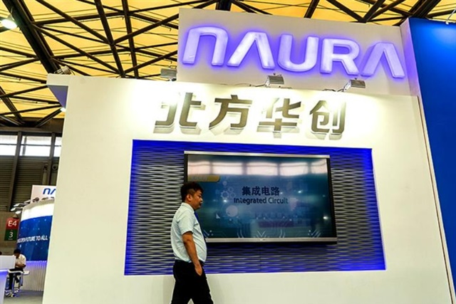
Naura Unveils First 600mm PLP Descum Tool for AI Chip Packaging
Naura, a player in the semiconductor manufacturing landscape, has recently unveiled a significant innovation in the field of packaging for artificial intelligence-dedicated chips. This development involves its first 600mm tool specifically designed for the "descum" process within Panel Level Packaging (PLP). This advancement underscores the increasing importance of advanced production phases to meet the demand for increasingly sophisticated AI hardware.
The announcement, reported by Yicai, positions Naura as a key supplier in a crucial technological segment for the expansion of AI computing capabilities globally. Efficiency and scalability in chip packaging are decisive factors for the availability and final cost of components that power Large Language Models (LLM) and other artificial intelligence applications.
Technical Detail and Implications
At the core of the announcement is the 600mm tool for PLP descum. Panel Level Packaging is a technique that allows multiple chips to be processed simultaneously on a larger substrate (a "panel"), rather than on individual wafers. This approach aims to improve manufacturing efficiency and reduce per-unit costs, a fundamental aspect for the mass production of high-tech components.
The "descum" process is a critical step in semiconductor fabrication, involving the removal of organic or polymeric residues after lithography, ensuring the necessary cleanliness for subsequent deposition and interconnection phases. The introduction of a 600mm machine for this operation indicates Naura's capability to handle high volumes and larger formats, essential for the mass production of complex AI chips, such as GPUs or dedicated accelerators, which require advanced packaging to maximize performance and energy efficiency.
Context and Relevance for AI-RADAR
For companies evaluating on-premise deployment strategies for their AI and LLM workloads, hardware availability and cost are decisive factors. Innovations in chip packaging, like the one proposed by Naura, can directly impact the global supply chain of critical components. Greater efficiency in AI chip production can translate into better availability of GPUs and other accelerators, potentially influencing the overall Total Cost of Ownership (TCO) for self-hosted infrastructures.
The ability to produce chips more economically and at scale is fundamental to lowering entry barriers and supporting the growth of private data centers and air-gapped solutions, where data sovereignty and hardware control are paramount. For those evaluating on-premise deployments, there are trade-offs between initial costs, scalability, and control, and hardware availability is a key element in this equation.
Future Outlook
Naura's entry into this specific segment of advanced packaging highlights a broader trend in the semiconductor industry: the optimization of every production phase to support the explosion of artificial intelligence. As the demand for AI computing power continues to grow exponentially, innovation is not limited solely to chip design but also extends to manufacturing and packaging processes.
This type of development can contribute to diversifying the supply chain and mitigating risks associated with reliance on a limited number of suppliers, a crucial aspect for the resilience of AI infrastructures globally. The ability to handle large panels like 600mm is a step forward towards more efficient and scalable production, essential for sustaining the next generation of AI innovations.


💬 Comments (0)
🔒 Log in or register to comment on articles.
No comments yet. Be the first to comment!