Introduzione
La crescente domanda di potenza di calcolo per i carichi di lavoro di intelligenza artificiale, in particolare per i Large Language Models (LLM), spinge l'industria a esplorare soluzioni innovative a ogni livello della catena di produzione. In questo contesto, due attori chiave nel settore dei materiali e dei display, BOE e Corning, stanno concentrando i loro sforzi sullo sviluppo di substrati in vetro per il packaging dei chip AI. Questa iniziativa segna un potenziale passo avanti nella progettazione e produzione di processori dedicati all'AI, con implicazioni significative per le future infrastrutture.
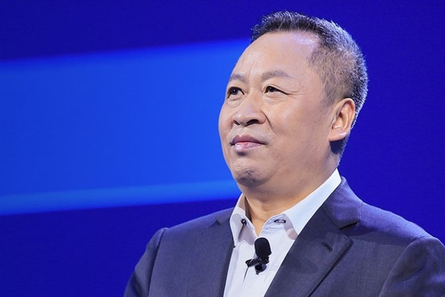
L'annuncio, che vede coinvolto il presidente di BOE, Chen Yanshun, evidenzia un interesse strategico verso materiali alternativi per migliorare le prestazioni e l'efficienza dei componenti hardware. L'obiettivo è superare i limiti delle tecnicie di packaging attuali, che spesso rappresentano un collo di bottiglia per l'integrazione di un numero sempre maggiore di transistor e memorie ad alta larghezza di banda.
Il Potenziale dei Substrati in Vetro per il Packaging AI
I substrati in vetro rappresentano una promettente alternativa ai tradizionali substrati organici o ai più complessi interposer in silicio. La loro adozione nel packaging dei chip AI potrebbe offrire diversi vantaggi tecnici cruciali. Il vetro, infatti, permette di realizzare linee e spazi di interconnessione molto più fini rispetto ai materiali organici, consentendo una maggiore densità di I/O (input/output) e, di conseguenza, l'integrazione di più chiplet o memorie HBM (High Bandwidth Memory) in un unico package.
Oltre alla densità, il vetro offre eccellenti proprietà termiche e meccaniche. La sua stabilità dimensionale superiore riduce la deformazione durante i processi di produzione e l'operatività, migliorando l'affidabilità del package. Dal punto di vista elettrico, i substrati in vetro possono garantire una minore perdita di segnale e una migliore integrità del segnale a frequenze elevate, fattori essenziali per le comunicazioni ad alta velocità all'interno dei chip AI di nuova generazione.
Implicazioni per le Infrastrutture On-Premise
L'evoluzione del packaging dei chip AI ha un impatto diretto sulle decisioni di deployment per le aziende che scelgono soluzioni self-hosted o ibride. Un packaging più efficiente, reso possibile dai substrati in vetro, può tradursi in acceleratori AI con maggiore VRAM e capacità di calcolo per unità di spazio. Questo significa che le organizzazioni possono ottenere più potenza di elaborazione all'interno dei loro data center on-premise, ottimizzando l'utilizzo dello spazio rack e riducendo potenzialmente il TCO a lungo termine.
Per i CTO e gli architetti di infrastruttura, la possibilità di disporre di hardware più denso e performante è fondamentale per affrontare carichi di lavoro AI sempre più esigenti, mantenendo al contempo la sovranità dei dati e la compliance normativa. Ambienti air-gapped o con stringenti requisiti di sicurezza beneficiano enormemente di soluzioni che massimizzano la capacità di calcolo locale, riducendo la dipendenza da servizi cloud esterni. La maggiore efficienza termica e elettrica dei nuovi package potrebbe anche contribuire a contenere i consumi energetici, un aspetto critico per la sostenibilità e i costi operativi.
Prospettive Future e Sfide di Adozione
Sebbene il potenziale dei substrati in vetro sia notevole, la loro adozione su larga scala nel packaging dei chip AI richiederà un significativo investimento in ricerca e sviluppo, oltre a superare diverse sfide produttive. La maturazione delle tecnicie di fabbricazione, la gestione dei costi e l'integrazione in una pipeline di produzione consolidata saranno fattori determinanti. Tuttavia, l'impegno di aziende come BOE e Corning sottolinea la serietà con cui l'industria sta affrontando la necessità di innovare per sostenere la crescita esponenziale dell'AI.
Queste innovazioni nel campo dei materiali e del packaging sono cruciali per sbloccare le prossime generazioni di performance AI, sia per il training che per l'inference. Per le aziende che valutano il deployment di LLM e altri carichi di lavoro AI su infrastrutture on-premise, monitorare l'evoluzione di queste tecnicie è essenziale per pianificare investimenti futuri e garantire che le proprie architetture possano scalare efficacemente, bilanciando performance, costi e requisiti di sicurezza.


💬 Commenti (0)
🔒 Accedi o registrati per commentare gli articoli.
Nessun commento ancora. Sii il primo a commentare!