TSMC Boosts AI Chip Production with CoWoS and SoIC
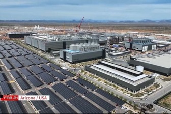
TSMC, the Taiwanese semiconductor manufacturing giant, has announced a significant expansion of its production capacity for advanced packaging technologies, specifically CoWoS (Chip-on-Wafer-on-Substrate) and SoIC (System-on-Integrated-Chips). This strategic move is a direct response to the explosion in global demand for AI accelerators, a sector largely driven by the rapid evolution and adoption of Large Language Models (LLMs).
TSMC's increased production capacity underscores the centrality of these advanced technologies for creating high-performance chips, which are indispensable for intensive workloads such as LLM training and inference. The availability of these components is a critical factor for companies planning investments in AI infrastructure, both in cloud environments and, increasingly, on-premise.
The Crucial Role of CoWoS and SoIC in the AI Era
CoWoS and SoIC technologies represent fundamental pillars in the architecture of modern AI accelerators. CoWoS, in particular, is a 3D packaging solution that allows for tight integration between the logic die (such as a GPU) and high-bandwidth memory (HBM). This vertical integration drastically reduces communication distances, improving memory bandwidth and lowering latency, which are essential factors for the efficient processing of enormous datasets and complex models.
SoIC, on the other hand, is an even more advanced integration technology that enables chip stacking directly at the wafer level. This approach offers even greater transistor density and performance, paving the way for more compact and energy-efficient systems. Both technologies are vital for overcoming the physical limitations of traditional planar architectures, allowing for the creation of chips with the VRAM and computing capacity required for the latest generation of AI models.
Implications for On-Premise Deployments and TCO
TSMC's capacity expansion has direct implications for organizations evaluating or implementing on-premise LLM deployments. The availability of a greater number of chips with advanced packaging means a potential improvement in the supply of high-end GPUs, such as those used for training and inference of complex models. Historically, the scarcity of these components has represented a significant bottleneck, influencing delivery times and costs.
For CTOs, DevOps leads, and infrastructure architects, increased availability can translate into better CapEx planning and a more favorable Total Cost of Ownership (TCO) analysis for self-hosted AI infrastructures. The ability to keep data and models within their own infrastructure boundaries, ensuring data sovereignty and regulatory compliance, largely depends on access to high-performance and reliable hardware. For those evaluating on-premise deployments, AI-RADAR offers analytical frameworks on /llm-onpremise to assess the trade-offs between costs, performance, and security requirements.
Future Outlook and the Race for Innovation
TSMC's commitment to expanding its advanced packaging capabilities reflects a long-term vision for the unstoppable growth of the AI market. However, the demand for computing power continues to outpace supply, pushing the entire technology supply chain to constantly innovate. The challenge is not only to produce more chips but also to make them more efficient, reducing energy consumption and environmental footprint.
As the industry moves towards increasingly complex and integrated architectures, the role of companies like TSMC becomes even more critical. The ability to provide cutting-edge components will determine the speed at which innovations in LLMs and AI in general can be implemented on a large scale, both in cloud environments and in private and air-gapped infrastructures, ensuring companies full control over their digital assets.


💬 Comments (0)
🔒 Log in or register to comment on articles.
No comments yet. Be the first to comment!