The Evolution of AI Packaging: TSMC's Vision
The artificial intelligence sector, particularly Large Language Models (LLMs), constantly pushes the boundaries of computational capabilities and hardware density. In this context, advanced chip packaging emerges as a critical factor for innovation. TSMC, a global leader in semiconductor manufacturing, recently shared its roadmap for next-generation packaging, focusing on processors for High-Performance Computing (HPC) and AI.
This roadmap reveals a clear strategy: on one hand, optimizing existing technologies; on the other, exploring future solutions that promise greater scalability. Decisions in this area directly impact data center design, power requirements, and ultimately, the Total Cost of Ownership (TCO) for companies implementing self-hosted AI infrastructures.
CoWoS: The Current Pillar for AI Processors
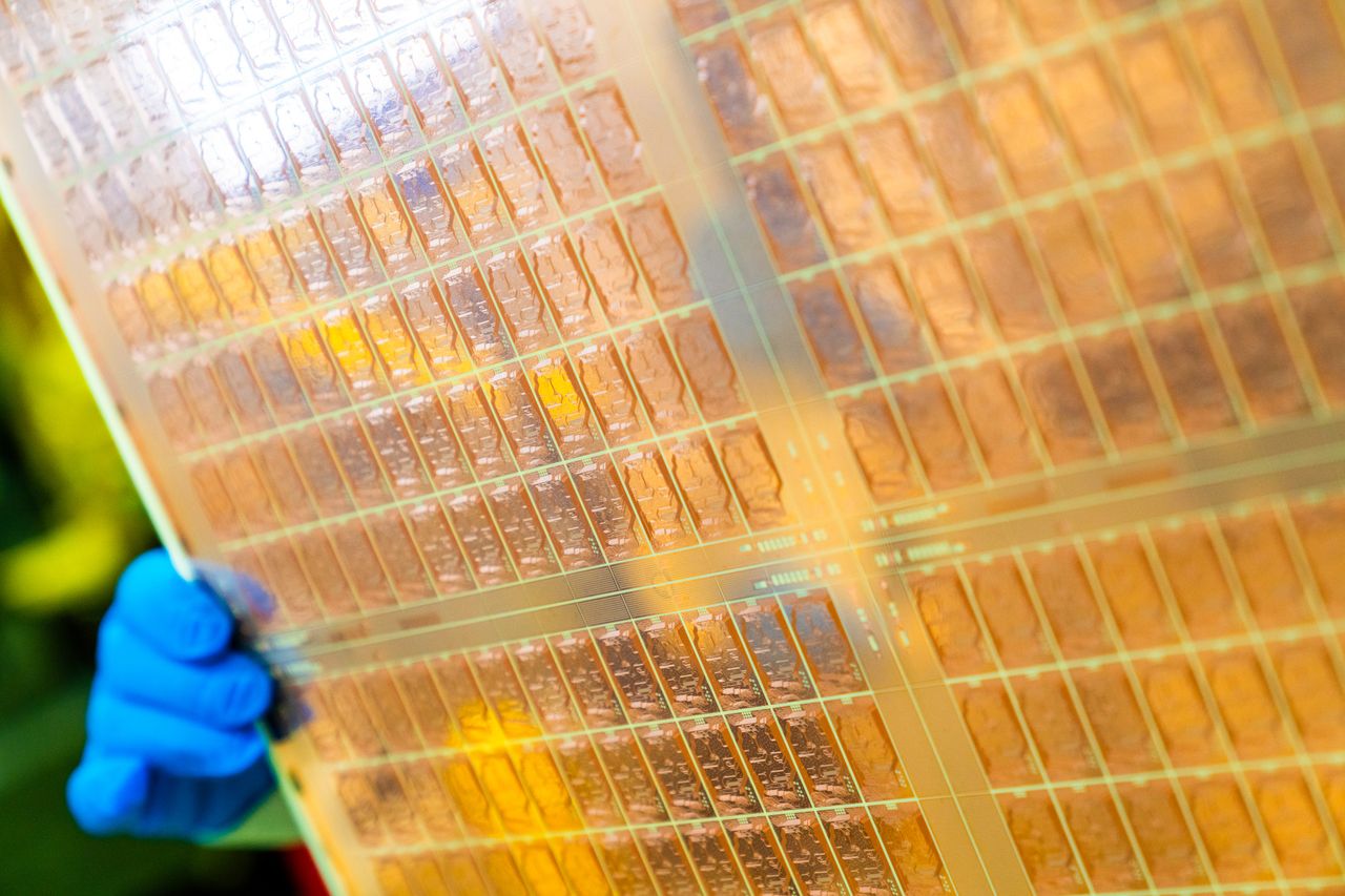
Currently, CoWoS (Chip-on-Wafer-on-Substrate) technology represents the core of TSMC's advanced packaging solutions for high-end AI chips. This technology, considered mature, is available in various forms – CoWoS-S, CoWoS-R, and CoWoS-L – each optimized for specific interconnection and integration needs.
Despite its effectiveness, CoWoS has inherent limitations that define its scope. TSMC's roadmap indicates a maximum limit of 12 reticles, the ability to integrate up to 8 HBM (High Bandwidth Memory) stacks, and an interposer with maximum dimensions of 80x80mm. These constraints are fundamental for system architects who must balance performance, memory capacity, and physical footprint when implementing on-premise AI clusters.
Panel Packaging: The Promise of Future Scalability
Looking ahead, TSMC is significantly investing in Panel Packaging, a technology that includes variants such as InFO_SoW, InFO_PoP, and InFO_LSI. The Panel Packaging approach stands out for its panel-level processing, which allows for the creation of significantly larger packages compared to CoWoS. This innovation paves the way for unprecedented scalability, with the ability to integrate up to 58 massive dies into a single package.
However, TSMC's roadmap clarifies a crucial aspect: Panel Packaging is not intended to replace CoWoS for the largest future AI processors anytime soon. While it offers advantages in terms of density and package size, its maturity and integration into production pipelines require time. This means that for the most demanding AI architectures, CoWoS will continue to be the reference technology for the foreseeable future.
Implications for On-Premise AI Deployments
TSMC's advanced packaging choices have profound implications for companies evaluating or managing on-premise AI deployments. The integration density offered by CoWoS and, prospectively, by Panel Packaging, directly influences the amount of computing power that can be housed in a single server or rack. This is crucial for optimizing data center space, reducing operational costs related to power and cooling, and ensuring data sovereignty in air-gapped environments.
For CTOs, DevOps leads, and infrastructure architects, understanding these dynamics is essential for long-term planning. The availability of chips with advanced packaging determines the ability to run LLM inference and training workloads efficiently and with control. While Panel Packaging promises a future of greater scalability, the current predominance of CoWoS means that hardware procurement strategies must continue to consider its specifications and limitations. AI-RADAR offers analytical frameworks on /llm-onpremise to evaluate the trade-offs between different hardware architectures and deployment strategies.


💬 Comments (0)
🔒 Log in or register to comment on articles.
No comments yet. Be the first to comment!