BOE Technology, a Chinese giant best known for display panels, is moving in an unexpected direction: chip packaging for artificial intelligence. According to Jiemian News, the company is betting on optical interconnects based on Micro LEDs and co‑packaged optics (CPO) on a glass substrate. This is not a simple product line extension, but an entry into a field where bandwidth density and energy efficiency are everything – because they directly shape the performance of AI systems, whether in the cloud or in on‑premise machine rooms.
Micro LEDs and glass: the building blocks of new packaging
Using Micro LEDs as light sources for chip‑to‑chip optical interconnection is a fascinating idea. Unlike traditional copper traces, an optical link can carry far more data per unit of energy over distances of a few centimeters – typical inside a server or between GPUs in a multi‑accelerator system. Micro LEDs, with their minuscule size and decent electro‑optical conversion efficiency, become candidates for embedding light beams directly into the chip package, eliminating electrical bandwidth bottlenecks.
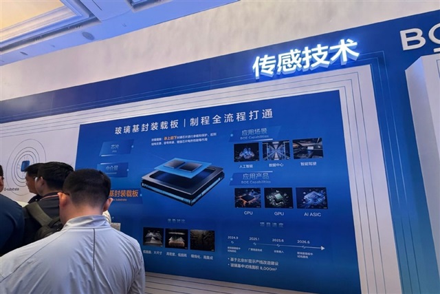
The glass substrate is the other key ingredient. Long explored as an alternative to silicon for interposers – the interconnection layers that connect multiple chiplets in a single package – glass offers a smoother surface, lower dielectric losses, and better thermal management at equivalent scale. Advanced variants like TGV (Through‑Glass Vias) substrates enable more efficient power delivery and signal routing, reducing overall complexity. Leveraging its experience handling large glass sheets for displays, BOE could find a competitive edge in a market where packaging cost and scalability are often the true gating factors.
Why AI needs optical packaging
The race toward ever‑larger LLMs and models is pushing current infrastructure to its limits. GPUs and specialized accelerators generate enormous data traffic, both internally and toward memory and other chips. Even high‑speed electrical links like NVLink or Infinity Fabric consume power proportionally to bandwidth and complicate server thermal design.
Optical packaging promises to decouple bandwidth and power: light‑based signaling can reach much higher communication densities without a dramatic jump in energy consumption. Furthermore, glass substrates reduce interference and improve signal integrity, crucial at high frequencies. For those evaluating on‑premise deployment, these are not academic niceties: an AI server that dissipates less heat and communicates faster among its components allows higher compute density per rack, lowers TCO, and simplifies thermal management in a data center.
Unknowns and outlook
No public technical specifications or production timelines are available yet. The project is likely still in research and development. While integrated optics is not new – competitors like Ayar Labs and semiconductor giants are exploring similar paths – a player like BOE with large‑scale manufacturing know‑how could accelerate industrialization.
A display company’s interest in AI packaging highlights a broader phenomenon: the convergence between panel fabrication and advanced semiconductor technologies. Glass, Micro LEDs, and photonics meet at a point that could redefine the architecture of future compute systems. For AI infrastructure operators, the signal is clear: innovation comes not only from chip process nodes, but also from how those chips are assembled and made to communicate. And in a world where data sovereignty drives toward local and hybrid deployments, every hardware efficiency gain translates into greater autonomy and control.


💬 Comments (0)
🔒 Log in or register to comment on articles.
No comments yet. Be the first to comment!