Introduction to the Era of 2D Transistors
The semiconductor industry is constantly seeking new frontiers to overcome the physical limits imposed by current technologies. In this context, the collaboration between giants like TSMC, ASML, and the research center Imec represents a strategic initiative to push 2D transistors towards mass production. This joint effort aims to revolutionize how chips are designed and manufactured, paving the way for a new generation of more powerful and efficient devices.
Transistor miniaturization has been the primary driver of technological progress for decades, but current architectures, such as FinFETs, are approaching their physical boundaries. The introduction of 2D transistors, based on atomic-thickness materials, offers a potential solution to these challenges, promising higher integration densities and improved energy performance—critical factors for the future of electronics.
The Challenge and Potential of 2D Transistors
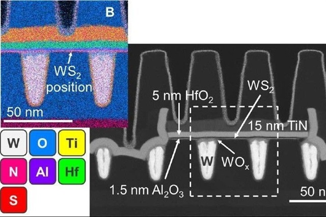
2D transistors utilize materials like molybdenum disulfide (MoS2) or tungsten diselenide (WSe2), which allow for extremely thin conductive channels, at the level of a few atoms. This characteristic enables more precise control over current flow and reduces losses, fundamental elements for increasing the energy efficiency of chips. The transition from three-dimensional to two-dimensional structures is complex and requires significant innovation at every stage of the production process.
The collaboration between TSMC, ASML, and Imec is crucial for addressing these challenges. Imec, with its expertise in advanced material and manufacturing process research and development, is exploring the fundamental properties of 2D materials. ASML, the world leader in lithography machines, is essential for developing the techniques needed to print nanoscale circuits with these new materials. TSMC, the world's largest semiconductor manufacturer, is tasked with translating these discoveries into scalable and reliable production processes, bringing innovation from the lab to the factory floor.
Implications for AI Hardware and On-Premise Deployments
The advancement of 2D transistors has direct and profound implications for the artificial intelligence sector, particularly for hardware dedicated to Large Language Models (LLM). Denser and more efficient chips translate into GPUs and AI accelerators with greater computing power and, potentially, higher VRAM and improved throughput, all while maintaining the same footprint or power consumption. This is a decisive factor for those evaluating on-premise LLM deployments.
For companies opting for self-hosted solutions, the availability of higher-performing and lower-power hardware can significantly reduce the Total Cost of Ownership (TCO). Superior energy efficiency lowers operational costs, while increased computing density allows for running larger models or more inference instances on fewer servers, optimizing space and infrastructure management. Furthermore, the ability to keep data and AI workloads within physical boundaries strengthens data sovereignty and regulatory compliance, which are priority aspects for many industries. For those evaluating on-premise deployments, AI-RADAR offers analytical frameworks on /llm-onpremise to assess the trade-offs between performance, costs, and control.
Future Prospects and Technological Challenges
While the potential of 2D transistors is enormous, the path to mass production is still long and fraught with challenges. The large-scale reproducibility of 2D materials, integration with existing manufacturing processes, and defect management at the atomic level are just some of the complexities that TSMC, ASML, and Imec must address. However, the collaborative nature of this effort indicates a clear strategic direction for the industry towards radical innovation.
The success of this initiative could not only extend Moore's Law but also redefine the capabilities of AI hardware, making on-premise inference and training systems even more competitive compared to cloud alternatives. Companies planning their AI infrastructures will need to closely monitor these developments, as innovations in silicon will directly determine the performance, efficiency, and TCO of future self-hosted solutions.


💬 Comments (0)
🔒 Log in or register to comment on articles.
No comments yet. Be the first to comment!